RHFLVDS325
Rad-hard quad LVDS receiver
Datasheet - production data
Large input common mode: -1 V to +4 V
Guaranteed up to 300 krad TID
SEL immune up to 135 MeV.cm²/mg
SET/SEU immune up to 32 MeV.cm²/mg
Description
The RHFLVDS325 is a quad, low-voltage
differential signaling (LVDS) receiver specifically
designed, packaged and qualified for use in
aerospace environments in a low-power and fast
data transmission standard.
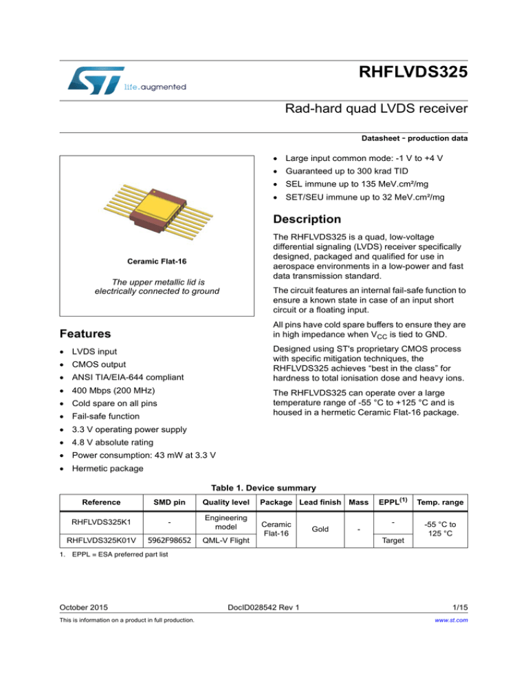
Ceramic Flat-16
The upper metallic lid is
electrically connected to ground
The circuit features an internal fail-safe function to
ensure a known state in case of an input short
circuit or a floating input.
All pins have cold spare buffers to ensure they are
in high impedance when VCC is tied to GND.
Features
Designed using ST's proprietary CMOS process
with specific mitigation techniques, the
RHFLVDS325 achieves “best in the class” for
hardness to total ionisation dose and heavy ions.
LVDS input
CMOS output
ANSI TIA/EIA-644 compliant
400 Mbps (200 MHz)
The RHFLVDS325 can operate over a large
temperature range of -55 °C to +125 °C and is
housed in a hermetic Ceramic Flat-16 package.
Cold spare on all pins
Fail-safe function
3.3 V operating power supply
4.8 V absolute rating
Power consumption: 43 mW at 3.3 V
Hermetic package
Table 1. Device summary
Reference
SMD pin
Quality level
RHFLVDS325K1
-
Engineering
model
RHFLVDS325K01V
5962F98652
QML-V Flight
Package Lead finish Mass
Ceramic
Flat-16
Gold
-
EPPL(1)
Temp. range
-
-55 °C to
125 °C
Target
1. EPPL = ESA preferred part list
October 2015
This is information on a product in full production.
DocID028542 Rev 1
1/15
www.st.com
Contents
RHFLVDS325
Contents
1
Functional description . . . . . . . . . . . . . . . . . . . . . . . . . . . . . . . . . . . . . . . 3
2
Pin configuration . . . . . . . . . . . . . . . . . . . . . . . . . . . . . . . . . . . . . . . . . . . . 4
3
Maximum ratings and operating conditions . . . . . . . . . . . . . . . . . . . . . . 5
4
Radiation . . . . . . . . . . . . . . . . . . . . . . . . . . . . . . . . . . . . . . . . . . . . . . . . . . 6
5
Electrical characteristics . . . . . . . . . . . . . . . . . . . . . . . . . . . . . . . . . . . . . 7
6
Test circuit . . . . . . . . . . . . . . . . . . . . . . . . . . . . . . . . . . . . . . . . . . . . . . . . . 9
7
Package information . . . . . . . . . . . . . . . . . . . . . . . . . . . . . . . . . . . . . . . . 11
7.1
Ceramic Flat-16 package information . . . . . . . . . . . . . . . . . . . . . . . . . . . 12
8
Ordering information . . . . . . . . . . . . . . . . . . . . . . . . . . . . . . . . . . . . . . . 13
9
Shipping information . . . . . . . . . . . . . . . . . . . . . . . . . . . . . . . . . . . . . . . 13
10
Revision history . . . . . . . . . . . . . . . . . . . . . . . . . . . . . . . . . . . . . . . . . . . 14
2/15
DocID028542 Rev 1
RHFLVDS325
1
Functional description
Functional description
Figure 1. Logic diagram and logic symbol
*
*
$
%
$
%
$
%
$
%
* *
$
%
%.
<
<
$
%
<
$
<
%
<
<
<
$
%
<
&6
Table 2. Truth table
Differential inputs
Enables
A, B
VID ≥100 mV
-100 mV < VID < 100 mV
VID ≤-100 mV
X
Open/Short or terminated
Note:
Output
G
G
Y
H
X
H
X
L
H
H
X
?
X
L
?
H
X
L
X
L
L
L
H
Z
H
X
H
X
L
H
1
The G input features an internal pull-up network. The G input features an internal pull-down
network. If they are floating the circuit is enabled.
2
Vid = VIA-VIB
3
L = low level, H = high Level, X = irrelevant, Z = high impedance (off). ? = intermediate
DocID028542 Rev 1
3/15
15
Pin configuration
2
RHFLVDS325
Pin configuration
Figure 2. Pin connections (top view)
Table 3. Pin description
4/15
Pin number
Symbol
Name and function
2, 6, 10, 14
1A to 4A
Receiver inputs
1, 7, 9, 15
1B to 4B
Negated receiver inputs
3, 5, 11, 13
1Y to 4Y
Receiver outputs
4
G
12
G
8
GND
Ground
16
VCC
Supply voltage
DocID028542 Rev 1
Enable
RHFLVDS325
3
Maximum ratings and operating conditions
Maximum ratings and operating conditions
Absolute maximum ratings are those values beyond which damage to the device may occur.
Functional operation under these conditions is not implied.
Table 4. Absolute maximum ratings
Symbol
VCC
Vi
Parameter
Supply voltage
Value
(1)
4.8
TTL inputs (operating or cold-spare)
-0.3 to 4.8
VOUT
TTL outputs (operating or cold-spare)
-0.3 to 4.8
VCM
LVDS common mode (operating or cold-spare)
Tstg
Storage temperature range
Tj
Unit
V
-2 to +5
-65 to +150
Maximum junction temperature
°C
+150
Rthjc
Thermal resistance junction to case(2)
22
°C/W
ESD
HBM: Human body model
– All pins excepted LVDS inputs
– LVDS inputs vs. GND
2
8
kV
500
V
CDM: Machine model
1. All voltages, except differential I/O bus voltage, are with respect to the network ground terminal.
2. Short-circuits can cause excessive heating. Destructive dissipation can result from short-circuits on the
amplifiers.
Table 5. Operating conditions
Symbol
Parameter
Min.
Typ.
Max.
3
3.3
3.6
VCC
Supply voltage
VCM
Static common mode on the receiver
-1
+4
Ambient temperature range
-55
+125
TA
DocID028542 Rev 1
Unit
V
°C
5/15
15
Radiation
4
RHFLVDS325
Radiation
Total dose (MIL-STD-883 TM 1019)
The products guaranteed in radiation within the RHA QML-V system fully comply with the
MIL-STD-883 TM 1019 specification.
The RHFLVDS325 is RHA QML-V, tested and characterized in full compliance with the
MIL-STD-883 specification, between 50 and 300 rad/s only (full CMOS technology).
All parameters provided in Table 7: Electrical characteristics apply to both pre- and postirradiation, as follows:
All test are performed in accordance with MIL-PRF-38535 and test method 1019 of
MIL-STD-883 for total ionizing dose (TID).
The initial characterization is performed in qualification only on both biased and
unbiased parts.
Each wafer lot is tested at high dose rate only, in the worst bias case condition, based
on the results obtained during the initial qualification.
Heavy ions
The behavior of the product when submitted to heavy ions is not tested in production.
Heavy-ion trials are performed on qualification lots only.
Table 6. Radiations
Type
TID
Heavy ions
6/15
Characteristics
Value
Unit
High-dose rate (50 - 300 rad/sec) up to:
300
krad
SEL immune up to:
(with a particle angle of 60 ° at 125 °C)
135
SEL immune up to:
(with a particle angle of 0 ° at 125 °C)
67
SET/SEU immune up to:
(at 25 °C)
32
DocID028542 Rev 1
MeV.cm²/mg
RHFLVDS325
5
Electrical characteristics
Electrical characteristics
In Table 7 below, VCC = 3 V to 3.6 V, capa-load (CL) = 10 pF, typical values are at
Tamb = +25 °C, min. and max values are at Tamb = - 55 °C and + 125 °C unless otherwise
specified
(
Symbol
Table 7. Electrical characteristics
Parameter
Test conditions
ICC
Total enabled supply current,
receivers enabled, not
switching
VID = 400 mV
ICCZ
Total disabled supply current,
receivers disabled
VID = 400 mV
G = GND and G = VCC
LVDS input power-off leakage
current(1)
VCC = 0 V, VIN = -1 V to 4 V
TTL I/O power-off leakage
current(1)
VCC = 0 V,
VIN, G and G = 3.6 V,
VOUT = 3.6 V
IOFF
Min.
-10
10
2
VCC
GND
0.8
10
IIH
High level input current
G and G inputs
VCC = 3.6 V, VIN = VCC
-10
Low level input current
G and G inputs
VCC = 3.6 V, VIN = 0
-10
VTL
Differential input low threshold
VCM = 1.2 V
VTH
Differential input high threshold VCM = 1.2 V
100
VCL
TTL input clamp voltage
ICL = 18 mA
-1.5
VID = 200 mVp-p
-1
G and G inputs
60
µA
Enable threshold low level
(2)
15
-60
VIL
Common mode voltage range
13
Unit
4
Enable threshold high level
VCMR
Max.
mA
VIH
IIL
Typ.
V
µA
10
-100
V
4
Common mode rejection
IID
Differential input current
VID = 400 mVp-p
-10
10
IICM
Common mode input current
VIC = - 1V to + 4V
-70
70
VOH
Output voltage high
IOH = -0.4 mA, VCC = 3 V
2.7
VOL
Output voltage low
IOL = 2 mA, VCC = 3 V
IOS
Output short-circuit current
VOUT = 0 V
-90
-30
mA
IOZ
Output tri-state current
Disabled, VOUT = 0 V or VCC
-10
10
µA
CIN
Input capacitance
On each LVDS input vs. GND
Rout
Output resistance
tPLHD
Propagation delay time, high to
VID = 200 mVp-p, input pulse
low output
from 1.1 V to 1.3 V, VCM = 1.2 V
Propagation delay time, low to Load: refer to Figure 3
high output
DocID028542 Rev 1
300
V
VCMREJ
tPHLD
F = 10 MHz
mV
mVp-p
0.25
1
µA
V
3
pF
45
3.5
ns
1
3.5
7/15
15
Electrical characteristics
RHFLVDS325
Table 7. Electrical characteristics (continued)
Symbol
Parameter
tSK1
Channel to channel skew
tSK2
Chip to chip skew(4)(5)
Test conditions
Min.
Typ.
(3)
(6)
Max.
Unit
0.6
VID = 200 mVp-p
Load: refer to Figure 3
3
tSKD
Differential skew
(tPHLD-tPLHD)
tPLZ
Propagation delay time, low
level to high impedance output
12
tPHZ
Propagation delay time, high
level to high impedance output
12
tPZH
Propagation delay time, high
impedance to high level output
tPZL
Propagation delay time, high
impedance to low level output
tD1
Fail-safe to active time
1
tD2
Active to fail-safe time
1
0.6
ns
Load: refer to Figure 4
12
12
µs
1. All pins except pin under test and VCC are floating.
2. Guaranteed by characterization on the bench.
3. tSK1 is the maximum delay time difference between all outputs of the same device (measured with all inputs connected
together).
4. tSK2 is the maximum delay time difference between outputs of all devices when they operate with the same supply voltage,
at the same temperature.
5. Guaranteed by design. tSKD is the maximum delay time difference between tPHLD-tPLHD
6. tSKD is the maximum delay time difference between tPHLD and tPLHD, see Figure 3.
Cold sparing
The RHFLVDS325 features a cold spare input and output buffer. In high reliability
applications, cold sparing enables a redundant device to be tied to the data bus with its
power supply at 0 V (VCC = GND) without affecting the bus signals or injecting current from
the I/Os to the power supplies. Cold sparing also allows redundant devices to be kept
powered off so that they can be switched on only when required. This has no impact on the
application. Cold sparing is achieved by implementing a high impedance between the I/Os
and VCC. The ESD protection is ensured through a non-conventional dedicated structure.
Fail-safe
In many applications, inputs need a fail-safe function to avoid an uncertain output state
when the inputs are not connected properly. In case of an LVDS input short circuit or floating
inputs, the TTL outputs remain in stable logic-high state.
8/15
DocID028542 Rev 1
RHFLVDS325
6
Test circuit
Test circuit
Figure 3. Timing test circuit and waveform
II
(A) IN+
VCM=(VIA+VIB)/2
VID
LVDS
Receiver
(B) IN-
VO
10pF
VIA
VIB
VIA
VIB
tPLHD
tPHLD
VO
VID=200mVp-p
50%
50%
80%
80%
20%
tf
20%
tr
1. All input pulses are supplied by a generator with the following characteristics: tr or tf ≤ 1 ns,
f = 1 MHz, ZO = 50 Ω, and duty cycle = 50%.
2. The product is guaranteed in test with CL = 10 pF
DocID028542 Rev 1
9/15
15
Test circuit
RHFLVDS325
Figure 4. Enable and disable time test circuit and waveform
Vcc
II
(A) IN+
VCM=(VIA+VIB)/2
VID
400 ohm
LVDS
Receiver
400 ohm
(B) IN-
VO
10pF
VIA
VIB
G
50%
50%
G
50%
50%
TPZH
TPHZ
VOH
VOH – 0.5V
VO
50%
high
Vcc/2
VO
Low
Vcc/2
TPLZ
TPZL
Vcc/2
Vcc/2
50%
VOL
VOL + 0.5V
1. All input pulses (including G and G) are supplied by a generator with the following characteristics:
tr or tf ≤ 1 ns, fG or fG = 500 kHz, and pulse width G or G = 500 ns.
2. The product is guaranteed in test with CL = 10 pF
10/15
DocID028542 Rev 1
RHFLVDS325
7
Package information
Package information
In order to meet environmental requirements, ST offers these devices in different grades of
ECOPACK® packages, depending on their level of environmental compliance. ECOPACK®
specifications, grade definitions and product status are available at: www.st.com.
ECOPACK® is an ST trademark.
DocID028542 Rev 1
11/15
15
Package information
7.1
RHFLVDS325
Ceramic Flat-16 package information
Figure 5. Ceramic Flat-16 package mechanical drawing
E
H
F
/
(
(
(
(
/
4
6
$
'
&V
1. The upper metallic lid is electrically connected to ground.
Table 8. Ceramic Flat-16 package mechanical data
Dimensions
Ref.
Millimeters
Min.
Max.
Min.
Typ.
Max.
A
2.31
2.72
0.091
0.107
b
0.38
0.48
0.015
0.019
c
0.10
0.18
0.004
0.007
D
9.75
10.13
0.384
0.399
E
6.75
7.06
0.266
0.278
E2
E3
4.32
0.170
0.76
e
12/15
Typ.
Inches
0.030
1.27
0.050
L
6.35
7.36
0.250
0.290
Q
0.66
1.14
0.026
0.045
S1
0.13
0.005
DocID028542 Rev 1
RHFLVDS325
8
Ordering information
Ordering information
Table 9. Order codes
Order code
Description
RHFLVDS325K1
Engineering
model
RHFLVDS325K01V
QML-V flight
Temp. range
Package
Marking(1)
Packing
-55 °C to
125 °C
Ceramic
Flat-16
RHFLVDS325K1
Strip
pack
TBD
1. Specific marking only. Complete marking includes the following:
- SMD pin (on QML-V flight only)
- ST logo
- Date code (date the package was sealed) in YYWWA (year, week, and lot index of week)
- QML logo (Q or V)
- Country of origin (FR = France).
Note:
Contact your ST sales office for information regarding the specific conditions for products in
die form and QML-Q versions.
9
Shipping information
Date code
The date code is structured as follows:
Engineering model: EM xyywwz
QML flight model: FM yywwz
Where:
x = 3 (EM only), assembly location Rennes (France)
yy = last two digits of the year
ww = week digits
z = lot index of the week
DocID028542 Rev 1
13/15
15
Revision history
10
RHFLVDS325
Revision history
Table 10. Document revision history
14/15
Date
Revision
21-Oct-2015
1
Changes
Initial release
DocID028542 Rev 1
RHFLVDS325
IMPORTANT NOTICE – PLEASE READ CAREFULLY
STMicroelectronics NV and its subsidiaries (“ST”) reserve the right to make changes, corrections, enhancements, modifications, and
improvements to ST products and/or to this document at any time without notice. Purchasers should obtain the latest relevant information on
ST products before placing orders. ST products are sold pursuant to ST’s terms and conditions of sale in place at the time of order
acknowledgement.
Purchasers are solely responsible for the choice, selection, and use of ST products and ST assumes no liability for application assistance or
the design of Purchasers’ products.
No license, express or implied, to any intellectual property right is granted by ST herein.
Resale of ST products with provisions different from the information set forth herein shall void any warranty granted by ST for such product.
ST and the ST logo are trademarks of ST. All other product or service names are the property of their respective owners.
Information in this document supersedes and replaces information previously supplied in any prior versions of this document.
© 2015 STMicroelectronics – All rights reserved
DocID028542 Rev 1
15/15
15


