DATA SHEET
AAT3691
Dual Input 1.6A Linear Charger with 28V OVP in a 3x4 TDFN Package
General Description
Features
The AAT3691 BatteryManager™ is an integrated single
cell Lithium-Ion (Li-Ion) battery charger IC, designed to
operate from USB ports, AC adapter inputs, or from a
cellular phone charger adapter up to an input voltage of
typical 6.75V. For increased safety, The AAT3691 also
includes over-voltage input protection (OVP) up to 28V.
• Dual Input USB and AC Adapter Input
▪ Programmable Constant Current from 100mA to
1.6A for ADP Charge
▪ Programmable Constant Current from 50mA to 0.5A
for USB Charge
• No Battery Present Input Detection
• 3.0V ~ 6.75V (typical) Input Voltage Range
• Over-Voltage Input Protection up to 28V
• High Level of Integration with Internal:
▪ Power Device
▪ Reverse Current Blocking
▪ Current Sensing
• Automatic Recharge Sequencing
• Fast Over-Voltage Protection Turn Off and Release
Turn On Time
• Full Battery Charge Auto Turn Off/Sleep Mode/Charge
Termination
• Charge Status Indicator
• Automatic Charge Reduction
• Automatic Trickle Charge for Battery Preconditioning
• Thermal Shutdown Protection
• Active Digital Thermal Loop Control
• Power On Reset and Soft Start
• Active Low Enable with Internal 200kΩ Resistor PullDown to GND
• 3x4mm TDFN Package
The AAT3691 precisely regulates battery charge voltage
and current for 4.2V Li-Ion battery cells. The charge
current can be programmed up to 1.6A for ADP charging
and 0.5A for USB charging by external resistors on the
ADPSET/USBSET pins. In the case of an over-voltage
condition of ADP or USB input power exceeding typical
6.75V, the internal series switch opens, blocking the
damage to the battery and charging circuitry.
The AAT3691 also includes a no-battery present input
(NOBAT). When the NOBAT indicates that no battery is
present, OVP block will prevent the input power from
passing through the OVP block and suspend the charging
function.
Battery charging status is continuously monitored for
fault conditions. In the event of a battery over voltage or
chip over thermal failure, the charger will automatically
shutdown, protecting the charging device, control system
and battery, until the fault condition is removed. The
open drain status monitor output pin (STAT) is adopted
to report battery charging activity by active low.
The AAT3691 comes in a thermally enhanced, spacesaving, Pb-free 16-pin 3x4 mm TDFN package and is
specified for operation over the -40°C to +85°C temperature range.
Applications
•
•
•
•
Digital Still Cameras
Mobile Phones
Personal Data Assistants (PDAs)
Other Li-Ion Battery Powered Devices
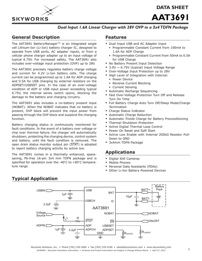
Typical Application
BATT+
USB
USBIN
Battery
Pack
BAT
1μF
10μF
USBCH
IC
BATT-
2.2μF
AAT3691
Voltage
Source
NOBAT
NOBAT
R
STAT
ADPIN
1μF
2.2μF
EN
ADP
USBSET
ADPCH
ADPSET
GND
ON/OFF
RADPSET
RUSBSET
Skyworks Solutions, Inc. • Phone [781] 376-3000 • Fax [781] 376-3100 • sales@skyworksinc.com • www.skyworksinc.com
201894B • Skyworks Proprietary Information • Products and Product Information are Subject to Change Without Notice. • April 27, 2012
1
DATA SHEET
AAT3691
Dual Input 1.6A Linear Charger with 28V OVP in a 3x4 TDFN Package
Pin Descriptions
Pin #
Name
Type
1
2.
3
4
5, 7, 10
6
8, 9
11
12
13
14
15
16
USB
USBCH
ADP
ADPCH
IC
STAT
GND
EN
ADPSET
USBSET
NOBAT
N/C
BAT
I
I/O
I
I/O
I
O
I
I
I
I
O
Function
Input from USB port connector
Output from USB OVP stage, input to battery charger. Decouple with 2.2μF capacitor.
Input from adapter port connector
Output from ADP OVP stage, input to battery charger. Decouple with 2.2μF capacitor.
Internally used. Connect to GND or leave floating.
Charge status indication pin, open drain.
Connect to power ground
Active low enable with internal 200kΩ resistor pull-down to GND.
ADP charge current programming input pin.
USB charge current programming input pin.
No battery present input. Logic “High“ indicates no battery. Internal 1.6MΩ pull-high resistor.
No connection.
Connect to lithium-ion battery.
Pin Configuration
TDFN34-16
(Top View)
USB
USBCH
ADP
ADPCH
IC
STAT
IC
GND
2
1
16
2
15
3
14
4
13
5
12
6
11
7
10
8
9
BAT
N/C
NOBAT
USBSET
ADPSET
EN
IC
GND
Skyworks Solutions, Inc. • Phone [781] 376-3000 • Fax [781] 376-3100 • sales@skyworksinc.com • www.skyworksinc.com
201894B • Skyworks Proprietary Information • Products and Product Information are Subject to Change Without Notice. • April 27, 2012
DATA SHEET
AAT3691
Dual Input 1.6A Linear Charger with 28V OVP in a 3x4 TDFN Package
Absolute Maximum Ratings1
Symbol
VADP ,VUSB
VADPCH,, VUSBCH
VN
TJ
TLEAD
Description
ADP, USB input continuous
Charger input continuous
BAT, STAT, EN, ADPSET , USBSET, NOBAT, IC
Operating Junction Temperature Range
Maximum Soldering Temperature (at Leads)
Value
Units
28
-0.3 to 7.5
-0.3 to 7.5 + 0.3
-40 to 150
300
V
V
V
C
C
Value
Units
50
2
C/W
W
Thermal Information2
Symbol
JA
PD
Description
Maximum Thermal Resistance (TDFN 3x4)
Maximum Power Dissipation
1. Stresses above those listed in Absolute Maximum Ratings may cause permanent damage to the device. Functional operation at conditions other than the operating conditions
specified is not implied. Only one Absolute Maximum Rating should be applied at any one time.
2. Mounted on a FR4 board.
Skyworks Solutions, Inc. • Phone [781] 376-3000 • Fax [781] 376-3100 • sales@skyworksinc.com • www.skyworksinc.com
201894B • Skyworks Proprietary Information • Products and Product Information are Subject to Change Without Notice. • April 27, 2012
3
DATA SHEET
AAT3691
Dual Input 1.6A Linear Charger with 28V OVP in a 3x4 TDFN Package
Electrical Characteristics1
VADP = VUSB = 5V, TA = -25°C to +85°C, unless otherwise noted. Typical values are at TA = 25°C.
Symbol
Description
Operation
VADP_MAX,
Input Over-Voltage Protection Range
VUSB_MAX
ADP and USB Normal Operating Input Voltage
VADP, VUSB
Range
IADP_OP,
Operating Current
IUSB_OP
ISD(OFF)
Shutdown Supply Current
ISTANDBY
Standby Mode Current
Leakage Current from BAT Pin
IBAT
Over-Voltage Protection
Over-Voltage Protection Trip Voltage
VOVPT
Hysteresis
Battery Charger
VUVLO_ADP, Under-Voltage Lockout Threshold
VUVLO_USB
UVLO Hysteresis
Voltage Regulation
VBAT_EOC
Output Charge Voltage Regulation
VCH/VCH Output Charge Voltage Tolerance
VMIN
Preconditioning Voltage Threshold
VRCH
Conditions
Min
3.0
VADP or VUSB = 5V, Charge current =
100mA, EN = 0V
VADP or VUSB = 5V, EN = 5V
Charge Terminated
VBAT = 4V, USB and ADP open
Rising edge
0.5
8
300
1
6.5
6.75
300
Rising edge
Max
Units
28
V
6.5
V
1.5
mA
4
μA
μA
μA
7.0
V
mV
3.0
V
mV
4.242
V
%
V
150
4.158
2.4
Battery Recharge Voltage Threshold
Battery Charging Device
Charging and OVP Total ON Resistance
RDS(ON)
Current Regulation
ADP Charge Current Programmable Range
ILIM_ADP
ILIM_USB
USB Charge Current Programmable Range
ICH_CC
Constant-Current Mode Charge Current
VADPSET,
ADPSET, USBSET Pin Voltage
VUSBSET
KIADPSET
Charge Current Set Factor: ICH_CC/IADPSET
KIUSBSET
Charge Current Set Factor: ICH_CC/IUSBSET
Typ
4.20
0.5
2.6
VBAT_EOC
- 0.1
VADP or VUSB = 5V, TA = 25°C
VBAT = 3.6V
100
50
-10
2.8
V
600
m
1600
500
10
mA
mA
%
2
Constant current mode, VBAT = 3.6V
Constant current mode, VBAT = 3.6V
V
800
800
ICH_TRK
Trickle Charge Current
RADPSET = 8k
5
10
15
ICH_TERM
Charge Termination Threshold Current
ICH_CC ≥ 800mA
8
10
12
%
ICH_CC
%
1. The AAT3691 is guaranteed to meet performance specifications over the -40°C to +85°C operating temperature range and are assured by design, characterization and correlation with statistical process controls.
4
Skyworks Solutions, Inc. • Phone [781] 376-3000 • Fax [781] 376-3100 • sales@skyworksinc.com • www.skyworksinc.com
201894B • Skyworks Proprietary Information • Products and Product Information are Subject to Change Without Notice. • April 27, 2012
DATA SHEET
AAT3691
Dual Input 1.6A Linear Charger with 28V OVP in a 3x4 TDFN Package
Electrical Characteristics (continued)1
VADP = VUSB = 5V, TA = -25°C to +85°C, unless otherwise noted. Typical values are at TA = 25°C.
Symbol
Description
Logic Control / Battery Protection
Input High Threshold
VEN#(H)
VEN#(L)
Input Low Threshold
VSTAT
Output Low Voltage
ISTAT
STAT Pin Current Sink Capability
VNOBAT(H)
No Battery Present Input High Threshold
VNOBAT(L)
No Battery Present Input Low Threshold
VBOVP
Battery Over-Voltage Protection Threshold
TRESPOV
Over-Voltage Response Time
TOVPON
OVP Switch OVP Release Turn-On Delay Time
TOVPSTARTON
OVP Switch Start Up Turn-On Delay Time
TOVPR
OVP Switch Turn-On Rise Time
TSHDN
Chip Thermal Shutdown Temperature
Conditions
VADP = 5V
Min
Typ
Max
4
0.4
0.4
8
1.2
STAT pin sinks 4mA
1.2
0.4
4.4
VADP, VUSB voltage step up signal from 6V
to 8V
VADP voltage step down signal from 8V to
6V, RLOAD = 10, CADPCH = 1μF
VADP voltage step up signal from 0V to
5V, RLOAD = 10, CADPCH = 1μF
RLOAD = 10, CADPCH = 1μF
Thermal Shutdown Threshold
Hysteresis
0.5
1.0
Units
V
V
V
mA
V
V
V
μs
5
μs
130
μs
100
140
15
μs
°C
1. The AAT3691 is guaranteed to meet performance specifications over the -40°C to +85°C operating temperature range and are assured by design, characterization and correlation with statistical process controls.
Skyworks Solutions, Inc. • Phone [781] 376-3000 • Fax [781] 376-3100 • sales@skyworksinc.com • www.skyworksinc.com
201894B • Skyworks Proprietary Information • Products and Product Information are Subject to Change Without Notice. • April 27, 2012
5
DATA SHEET
AAT3691
Dual Input 1.6A Linear Charger with 28V OVP in a 3x4 TDFN Package
Typical Characteristics
Over-Voltage Protection vs. Temperature
End of Charge Voltage vs. Supply Voltage
(RADPSET = 1kΩ, RUSBSET = 3.2kΩ)
4.22
6.80
4.21
6.70
6.65
Power sweep low to high
Power sweep high to low
6.60
VEOC (V)
VADP or VUSB (V)
6.75
4.20
4.19
6.55
USB
ADP
6.50
-40
-20
0
20
40
60
4.18
4.4
80
4.8
5.2
Temperature (°C)
ICHARGE vs. RADPSET
6.0
6.4
6.8
ICHARGE vs. RUSBSET
10000
1000
ICHARGE (mA)
ICHARGE (mA)
5.6
VADP or VUSB (V)
1000
100
10
100
10
1
10
100
1
10
RADPSET (kΩ)
100
RUSBSET (kΩ)
Battery Recharge Voltage Threshold
vs. Supply Voltage
Battery Recharge Voltage Threshold
vs. Temperature
(RADPSET = 1kΩ; RUSBSET = 3.2kΩ; CBAT = 22μF)
(VADP = VUSB = 5V; RADPSET = 1kΩ; RUSBSET = 3.2kΩ; CBAT = 22μF)
4.10
4.10
4.08
VRCH (V)
VRCH (V)
4.08
4.06
4.04
4.02
4.06
4.04
4.00
USB
ADP
3.98
3.96
4.5
4.9
5.3
5.7
VADP or VUSB (V)
6
6.1
6.5
4.02
4.00
-40
USB
ADP
-20
0
20
40
60
Temperature (°C)
Skyworks Solutions, Inc. • Phone [781] 376-3000 • Fax [781] 376-3100 • sales@skyworksinc.com • www.skyworksinc.com
201894B • Skyworks Proprietary Information • Products and Product Information are Subject to Change Without Notice. • April 27, 2012
80
DATA SHEET
AAT3691
Dual Input 1.6A Linear Charger with 28V OVP in a 3x4 TDFN Package
Typical Characteristics
End of Charge Voltage vs. Temperature
Charge Current vs. Temperature
(RADPSET = 1kΩ; RUSBSET = 3.2kΩ)
(VADP = VUSB = 5V; VBAT = 3.6V;
RADPSET = 1kΩ; RUSBSET = 3.2kΩ)
4.22
1800
USB
ADP
1600
1400
ICH (mA)
VEOC (V)
4.21
4.20
1200
1000
800
600
4.19
400
ADP
USB
200
4.18
-40
-20
0
20
40
60
0
-40
80
-20
0
Temperature (°C)
20
40
60
80
Temperature (°C)
Charging Current vs. Battery Voltage
USB Charging Current vs. Supply Voltage
(VADP = VUSB = 5V; RADPSET = 1kΩ; RUSBSET = 3.2kΩ)
(RUSBSET = 3.2kΩ)
600
1800
ADP
USB
1600
500
ICH_USB (mA)
ICH (mA)
1400
1200
1000
800
600
400
400
300
200
VBAT = 3.3V
VBAT = 3.6V
VBAT = 3.9V
100
200
0
2.5
2.7
2.9
3.1
3.3
3.5
3.7
3.9
4.1
4.3
0
4.0
4.5
4.4
4.8
VBAT (V)
5.2
5.6
6.0
6.4
6.8
VUSB (V)
ADP Charging Current vs. Supply Voltage
USB Charging Current vs. Supply Voltage
(RADPSET = 1kΩ)
(RUSBSET = 3.2kΩ)
600
1800
1600
500
ICH_USB (mA)
ICH_ADP (mA)
1400
1200
1000
800
600
VBAT = 3.3V
VBAT = 3.6V
VBAT = 3.9V
400
200
0
4.0
4.4
4.8
5.2
5.6
VADP (V)
6.0
6.4
400
300
-40°C
0°C
25°C
50°C
85°C
200
100
6.8
0
4.0
4.4
4.8
5.2
5.6
6.0
6.4
6.8
VUSB (V)
Skyworks Solutions, Inc. • Phone [781] 376-3000 • Fax [781] 376-3100 • sales@skyworksinc.com • www.skyworksinc.com
201894B • Skyworks Proprietary Information • Products and Product Information are Subject to Change Without Notice. • April 27, 2012
7
DATA SHEET
AAT3691
Dual Input 1.6A Linear Charger with 28V OVP in a 3x4 TDFN Package
Typical Characteristics
ADP Charging Current vs. Battery Voltage
USB Charging Current vs. Battery Voltage
(VADP = 5V)
(VUSB = 5V)
1800
600
RSET = 1kΩ
RSET = 1.14kΩ
RSET = 1.33kΩ
RSET = 1.6kΩ
RSET = 2kΩ
RSET = 3.2kΩ
RSET = 5.33kΩ
RSET = 16kΩ
1200
900
600
500
ICH_USB (mA)
ICH_ADP (mA)
1500
300
RSET = 3.2kΩ
RSET = 4kΩ
RSET = 5.33kΩ
RSET = 8kΩ
RSET = 16kΩ
RSET = 32kΩ
400
300
200
100
0
0
2.5
2.9
3.3
3.7
4.1
2.5
4.5
3.0
NOBAT High Input Threshold vs. Input Power
1.05
1.00
0.95
0.90
-40°C
25°C
85°C
3.6
4.2
4.8
5.4
6.0
NOBAT VIL (V)
NOBAT VIH (V)
0.65
1.10
0.85
0.60
0.55
0.50
-40°C
25°C
85°C
0.45
0.40
3.0
6.6
3.6
4.2
VUSB or VADP (V)
0.80
0.75
1.10
0.70
EN VIL (V)
EN VIH (V)
1.20
1.05
1.00
0.95
0.90
-40°C
25°C
85°C
0.85
4.8
5.2
5.6
VUSB or VADP (V)
5.4
6.0
6.6
Enable Input Low Threshold vs. Input Power
1.15
4.4
4.8
VUSB or VADP (V)
Enable Input High Threshold vs. Input Power
8
4.5
0.70
1.20
0.80
4.0
4.0
NOBAT Low Input Threshold vs. Input Power
1.15
0.80
3.0
3.5
VBAT (V)
VBAT (V)
6.0
6.4
0.65
0.60
0.55
0.50
-40°C
25°C
85°C
0.45
0.40
4.0
4.4
4.8
5.2
5.6
6.0
VUSB or VADP (V)
Skyworks Solutions, Inc. • Phone [781] 376-3000 • Fax [781] 376-3100 • sales@skyworksinc.com • www.skyworksinc.com
201894B • Skyworks Proprietary Information • Products and Product Information are Subject to Change Without Notice. • April 27, 2012
6.4
DATA SHEET
AAT3691
Dual Input 1.6A Linear Charger with 28V OVP in a 3x4 TDFN Package
Functional Block Diagram
Reverse Blocking
OVP Switch
BAT
USB
OVP Sense
and Control
CV/Precharge
USBCH
Current
Compare
USBSET
UVLO
Charge
Control
EN
Over-Temp.
Protect
NOBAT
IC
Current
Compare
ADPSET
STAT
ADPCH
Charge
Status
OVP Sense
and Control
GND
ADP
Reverse Blocking
Functional Description
The AAT3691 is a high performance battery charger
designed to charge single cell Lithium Ion or Polymer
batteries with up to 1600mA charging current from an
adaptor (ADP) power source, or with up to 500mA
charging current from an USB power source. The
AAT3691 is a stand-alone charging solution, with just a
few external component required for complete functionality. Both input paths include a fast turn-off over-voltage protection (OVP) circuit with voltage up to +28V and
an under-voltage lockout level of 3.0V.
The AAT3691 automatically selects the charging source
from USB or ADP according to ADP and USB voltage. The
ADP path is always the high priority charging path when
ADP voltage is higher than 4.5V. The charging current is
determined by the selected charging path and its external set resistor (RSET).
USB charging uses an automatic charge reduction loop
control allow battery charging with limited available current from a USB port while maintaining the regulated
port voltage. This system assures that the battery
charge function will not overload a USB port while charging if other system demands also share power with the
respective port supply.
During adapter charging, high set charging current or
high ambient operating temperature may cause the
AAT3691 junction temperature to rise up to 110°C. A
special digital thermal loop control system is employed
to maximize charging current by dynamically decreasing
the battery charging current.
Thermal protection shuts down the AAT3691's charging
function when internal dissipation becomes excessive,
while OVP function still works. The junction over-temperature threshold is 140°C with 15°C of hysteresis. Once
an over-temperature condition is removed, the charging
function automatically recovers.
The status monitor output pin (STAT) is designed to indicate the battery charge status with open-drain structure
by directly driving one external LED.
Battery Charging Operation
Regardless of which charge input function is selected
(adapter input or USB input), the AAT3691 has three
basic modes for the battery charge cycle: preconditioning (trickle) charge, constant current/fast charge, and
constant voltage charge. When no automatic charge
reduction mode or digital thermal loop is triggered, the
charge profile is controlled as shown in Figure 1.
Skyworks Solutions, Inc. • Phone [781] 376-3000 • Fax [781] 376-3100 • sales@skyworksinc.com • www.skyworksinc.com
201894B • Skyworks Proprietary Information • Products and Product Information are Subject to Change Without Notice. • April 27, 2012
9
DATA SHEET
AAT3691
Dual Input 1.6A Linear Charger with 28V OVP in a 3x4 TDFN Package
Battery Charge Current
Battery Voltage
Preconditioning
Trickle Charge
Phase
Constant Current
Charge Phase
Constant Voltage
Charge Phase
Charge Complete Voltage
I = Max CC
Regulated Current
Charge Current
Battery Voltage
Constant Current Mode
Voltage Threshold
Trickle Charge and
Termination Threshold
I = CC/10
Time
Figure 1: Charge Current vs. Battery Voltage Profile during Charging Phases.
Battery charging commences only after the AAT3691
checks several conditions in order to maintain a safe
charging environment. The input supply must be above
the minimum operating voltage and the enable pin must
be low. When the battery is connected to the BAT pin and
the NOBAT pin indicates there is a battery connected,
the AAT3691 checks the condition of the battery and
determines which charging mode to apply. If the battery
voltage is below VMIN, then the device begins trickle
charging by charging at 10% of the programmed constant current. For example, if the programmed current is
500mA, then the trickle charge current is 50mA. Trickle
charging is a safety precaution for a deeply discharged
cell and will also reduce the power dissipation in the
internal series pass MOSFET when the input-output voltage differential is at its highest. Trickle charging continues until the battery voltage reaches VMIN. At this point,
the AAT3691 begins constant current charging. The current value for this mode is programmed by the external
resistors from the ADPSET and USBSET pin to ground.
Programmed current can be set from a minimum of
100mA up to a maximum of 1.6A for an ADP power
source, and from a minimum of 50mA up to a maximum
of 500mA for a USB power source. Constant current
charging continues until the battery voltage reaches the
voltage regulation point, VBAT_EOC. When the battery voltage reaches VBAT_EOC (typical 4.2V), the AAT3691 will
switch to constant voltage mode. Constant current
charge will continue until the charging current is reduced
to 10% of the programmed current. After the charge
10
cycle is complete, the AAT3691 turns off the series pass
device and automatically goes into standby mode.
During this time, the series pass device will block current
in both directions, therefore preventing the battery from
discharging through the IC.
The AAT3691 remains in standby mode until either the
battery terminal voltage drops below the VRCH threshold,
the charger EN pin is recycled, or the charging source is
reconnected. In all cases, the AAT3691 will monitor all
parameters and resume charging in the most appropriate mode.
Over-Voltage Protection
In normal operation an OVP switch acts as a slew-rate
controlled load switch, connecting and disconnecting the
power supply from ADP to ADPCH and USB to USBCH. A
low-resistance MOSFET is used to minimize the voltage
drop between the voltage source and the charger and to
reduce the power dissipation. When the voltage on the
input exceeds the 6.75V (typical) voltage limit, the
device immediately turns off the internal OVP switch,
disconnecting the load from the abnormal voltage and
preventing damage to any downstream components.
On initial power-up with low and battery present, if
VUSB/ADP < VUVLO (3V maximum), the OVP switch is held
off; if VUVLO < VUSB/ADP < 6.75V (typical), the OVP switch
will turn on after a 130μs typical internal delay; if VUSB/ADP
rises above 6.75V (typical), the OVP switch is turned off
after a 0.5μs typical internal delay.
Skyworks Solutions, Inc. • Phone [781] 376-3000 • Fax [781] 376-3100 • sales@skyworksinc.com • www.skyworksinc.com
201894B • Skyworks Proprietary Information • Products and Product Information are Subject to Change Without Notice. • April 27, 2012
DATA SHEET
AAT3691
Dual Input 1.6A Linear Charger with 28V OVP in a 3x4 TDFN Package
System Operation Flowchart
Power On Reset
OVP Switch Off
Yes
NOBAT Indicates No
Battery
No
Enable
Adapter Charge
No
Yes
No
USBCH =
ADPCH = 0V
Preconditioning
Test
VMIN > VBAT
OVP (6.75V) ≥
V USB or VADP ≥
VUVLO_ADP or VUVLO_USB
(3V)
No
Yes
Preconditioning
(Trickle Charge)
Thermal Loop
Current
Reduction in
C.C. Mode
No
Yes
Yes
Recharge Test
VRCH > V BAT
Yes
Current Phase Test
VIN > VBAT_EOC
Yes
Constant
Current Charge
Mode
Device Thermal
Loop Monitor
TJ > 115°C
USBCH = USB,
ADPCH = ADP
No
No
VADPCH > VUVLO_ADPCH
(3.5V)
Voltage Phase Test
IBAT > ITERM
Yes
Yes
Constant
Voltage Charge
Mode
No
No
Charge Completed
No
VUSBCH > VUVLO_USBCH
(3.5V)
Yes
USB Charge
Preconditioning
Test
VMIN > VBAT
No
Yes
Preconditioning
(Trickle Charge)
Auto Charge
Reduction
Loop
Control
No
Yes
Recharge Test
VRCH > VBAT
Yes
Current Phase Test
VIN > VBAT_EOC
Yes
Constant
Current Charge
Mode
VUSBCH < 4.5V
No
No
Voltage Phase Test
IBAT > ITERM
Yes
Constant
Voltage Charge
Mode
No
Charge Completed
Skyworks Solutions, Inc. • Phone [781] 376-3000 • Fax [781] 376-3100 • sales@skyworksinc.com • www.skyworksinc.com
201894B • Skyworks Proprietary Information • Products and Product Information are Subject to Change Without Notice. • April 27, 2012
11
DATA SHEET
AAT3691
Dual Input 1.6A Linear Charger with 28V OVP in a 3x4 TDFN Package
Application Information
ICH_CC (mA)
50
75
100
200
300
400
500
600
700
800
900
1000
1100
1200
1300
1400
1500
1600
Charge Sources
The AAT3691 operates from sources of an adapter or
USB interface. The internal system control will always
select the adapter input to charge the battery rather
than the USB input if the adapter voltage is above 4.5V.
The normal charging input voltage range is up to typical
6.75V. The device can withstand up to 28V on the adapter or USB inputs without damage to the IC. If VADP or VUSB
is greater than 6.75V, the internal over-voltage protection circuitry disables charging until the input falls below
typical 6.55V.
AC Adapter/USB System Power Charging
Adapter Mode
In the adapter mode, constant current charge levels up
to 1.6A can be programmed by the user. The fast charge
current for the adapter input mode is set by the RADPSET
resistor connected between ADPSET and ground. It is
programmed by the following equations:
IADP_CC =
2
· KIADPSET
RADPSET
RADPSET =
2
· KIADPSET
IADP_CC
with KIADPSET = 800. Table 1 gives the recommended 1%
tolerance metal film resistance values for a desired constant current charge level.
The initial thermal loop current can be estimated by the
following equation:
ITLOOP = ICC · 0.44
12
RUSBSET (kΩ)
16
8.06
5.36
4.02
3.24
2.67
2.32
2
1.78
1.60
1.47
1.33
1.24
1.15
1.07
1
32.4
21.5
16
8.06
5.36
4.02
3.24
Table 1: Standard 1% Metal Film Resistor Values
for Constant Current Setting.
The thermal loop control re-evaluates the circuit die
temperature every three seconds and raises the fast
charge current in small steps to the full fast charge current level. Figure 2 illustrates the thermal loop function
at 1A fast charge current as the ambient temperature
increases and recovers. In this manner the thermal loop
controls the system charge level, and the AAT3691 provides the highest level of constant current in the fast
charge mode for any possible valid ambient temperature
condition.
1.6
Thermal Loop Control
1.4
Ambient Temperature increases
Charge Current (0.2A/div)
To protect the linear charging IC from thermal problems,
a special thermal loop control system is used to maximize charging current under adapter charge mode. The
thermal management system measures the internal circuit die temperature and reduces the fast charge current
when the die exceeds the preset internal temperature
control threshold. Once the thermal loop control becomes
active, the fast charge current is initially reduced by a
factor of 0.44.
RADPSET (kΩ)
1.2
1.0
0.8
0.6
0.4
Ambient Temperature decreases
0.2
0.0
Time (10s/div)
Figure 2: Digital Thermal Loop Function
at 1A Fast Charge Current with Ambient
Temperature Increasing and Recovering.
Skyworks Solutions, Inc. • Phone [781] 376-3000 • Fax [781] 376-3100 • sales@skyworksinc.com • www.skyworksinc.com
201894B • Skyworks Proprietary Information • Products and Product Information are Subject to Change Without Notice. • April 27, 2012
DATA SHEET
AAT3691
Dual Input 1.6A Linear Charger with 28V OVP in a 3x4 TDFN Package
Adapter Input Charge Inhabit and Resume
USB Input Charge Inhibit and Resume
The AAT3691 has an under-voltage lockout feature so
that if the charger input supply ADP pin drops below the
UVLO threshold, the charger will suspend charging.
When the UVLO condition is removed and VADPCH > VBAT,
the system charge control assesses the state of charge
of the battery cell and automatically resumes charging in
the appropriate phase (pre-conditioning trickle charge,
constant current charge, constant voltage charge or end
of charge) according to the condition of the battery.
The AAT3691 UVLO and power on reset feature functions
when the USB input pin voltage level drops below the
UVLO threshold. At this point, the charger suspends
charging and shuts down. When power is re-applied to
the USB pin or the UVLO condition recovers, the system
charge control will assess the state of charge on the battery cell and automatically resume charging in the
appropriate mode for the condition of the battery.
Enable / Disable
USB Mode
The AAT3691 also provides an input for intelligent USB
charging. When no voltage is present on the adapter
input pin or adapter input is below 4.5V, the charge controller will automatically switch to accepting power from
the USB input. The USB charge may be user programmed
to any level between 50mA and 500mA by selecting the
appropriate resistor values for RUSBSET.
IUSB_CC =
2
· KIUSBSET
RUSBSET
RUSBSET =
2
· KIUSBSET
IUSB_CC
Among them, KIUSBSET is 800. Refer to Table 1 for recommended RUSBSET values for the desired USB input constant
current charge levels.
USB Charge Reduction
In many instances, product system designers do not
know the real properties of a potential USB port used to
supply power to the battery charger. Typically, powered
USB ports found on desktop and notebook PCs should
supply up to 500mA. If a USB port being used to supply
the charger is unable to provide the programmed fast
charge current or if the system under charge must share
supply current with other functions, the AAT3691 automatically reduces USB fast charge current to maintain
port integrity and protect the host system.
The USB charge reduction system becomes active when
the voltage on the USBCH input falls below the USB
charge reduction threshold, typically 4.5V. The charge
reduction system reduces the fast charge current level in
a linear fashion until the voltage sensed on the USB input
recovers above the charge reduction threshold voltage.
The AAT3691 provides an enable function to allow the
normal operating input voltage to pass through and control the IC charging. The Enable (EN) pin is active low
and is pulled down to ground by an internal 200kΩ resistor. When pulled to a logic high level, the AAT3691 is
shut down and forced into the sleep state during which
input voltage up to 28V will be blocked and charging be
halted regardless of the battery voltage or charging
state. When the device is re-enabled, the OVP block will
automatically reassess the input voltage and allow the
normal operating voltage to pass through. If a battery is
also present (NOBAT is low), the charge control circuit
will automatically reset and resume charging with the
appropriate charging mode based on the battery charge
state and measured cell voltage.
Over-Temperature Shutdown
Thermal protection completely disables charging when
internal dissipation exceeds the junction over-temperature threshold, which is 140°C with 15°C of hysteresis.
Once the over-temperature fault condition is removed,
the charge function automatically recovers.
Battery Charge Status Indication
The AAT3691 has one status LED driver output. The LED
can indicate simple functions such as battery charging,
charge complete, and charge disabled.
Description
EN
LED Status
Battery charging
Charge complete
Charge disabled
low
low
high
on
off
off
Table 2. LED Status Conditions.
Skyworks Solutions, Inc. • Phone [781] 376-3000 • Fax [781] 376-3100 • sales@skyworksinc.com • www.skyworksinc.com
201894B • Skyworks Proprietary Information • Products and Product Information are Subject to Change Without Notice. • April 27, 2012
13
DATA SHEET
AAT3691
Dual Input 1.6A Linear Charger with 28V OVP in a 3x4 TDFN Package
Output Capacitor
The LED anodes should be connected to either VUSBCH or
VADPCH, depending upon the system design requirements.
The LEDs should be biased with as little current as necessary to create reasonable illumination; therefore, a
ballast resistor should be adopted to limit the current
flowing through the LED by connecting it with the LED in
series between STAT and VUSBCH or VADPCH. LED current
consumption will add to the overall thermal power budget for the device package, so LED drive current should
be kept to a minimum. 2mA should be sufficient to drive
most low-cost green or red LEDs. It is not recommended
to exceed 8mA for driving an individual status LED. The
required ballast resistor value can be estimated using
the following formulas:
The AAT3691 requires a 1μF ceramic capacitor on the
BAT pin to maintain circuit stability. This value should be
increased to 10μF or more if the battery connection is
made any distance from the charger output. In a fast
charge application with current above 1A, a 22μF output
capacitor is required to obtain an accurate recharge voltage threshold. If the AAT3691 is used in applications
where the battery can be removed from the charger,
such as in the case of desktop charging cradles, an output capacitor value greater than 10μF may be required
to prevent the device from cycling on and off when no
battery is present.
To connect to ADPCH:
Thermal Considerations
R=
VADPCH - VFLED
ILED
To connect to USBCH:
R=
VUSBCH - VFLED
ILED
For example, using a red LED with 2.0V VF @ 2mA, calculate R under 5.5V VADPCH:
R=
5.5V - 2.0V
= 1.75kΩ
2mA
Capacitor Selection
Input Capacitor
An input capacitor is used to filter the input voltage by
placing a decoupling capacitor between the ADP, ADPCH,
USB and USBCH pins and ground. An input capacitor in
the range of 1μF to 10μF is recommended. If the source
supply is unregulated, it may be necessary to increase
the capacitance to keep the input voltage above the
under-voltage lockout threshold during device enable
and when battery charging is initiated. This input capacitor range is also suitable for a system with an external
power supply source, such as a typical AC-to-DC wall
adapter. It will minimize switching or power bounce
effects when the power supply is “hot plugged”. Likewise,
a 2.2μF or greater input capacitor is recommended for
the USB input to help buffer the effects of USB source
power switching, noise, and input cable impedance.
14
The actual maximum charging current is a function of
the charge input voltage (USBCH and ADPCH), the battery voltage at the BAT pin, the ambient temperature,
the rising temperature when charge current passing
through the RDS(ON) of the charging pass, and the thermal
impedance of the package. The maximum programmable current may not be achievable under all operating
parameters.
The AAT3691 is offered in a 3x4mm TDFN package
which can provide up to 2.0W of power dissipation when
properly soldered to a printed circuit board and has a
maximum thermal resistance of 50°C/W. Many considerations should be taken into account when designing the
printed circuit board layout, as well as the placement of
the charger IC package in proximity to other heat generating devices in a given application design. The ambient temperature around the charger IC will also have an
effect on the thermal limits of a battery charging application. The maximum limits that can be expected for a
given ambient condition can be estimated by the following discussion:
First, the maximum power dissipation for a given situation should be calculated:
PD = [(VIN - VBAT) · ICC + (VIN · IOP)]
Where:
PD = Total power dissipation of the AAT3691
VIN = VADP or VUSB, depending on which mode is selected
VBAT = Battery voltage at the BAT pin
ICC = Maximum constant fast charge current programmed for the application
IOP = Quiescent current consumed by the charger IC
for normal operation.
Skyworks Solutions, Inc. • Phone [781] 376-3000 • Fax [781] 376-3100 • sales@skyworksinc.com • www.skyworksinc.com
201894B • Skyworks Proprietary Information • Products and Product Information are Subject to Change Without Notice. • April 27, 2012
DATA SHEET
AAT3691
Dual Input 1.6A Linear Charger with 28V OVP in a 3x4 TDFN Package
Next, the maximum operating ambient temperature for
a given application can be estimated based on the thermal resistance of the 3x4 TDFN package when sufficiently mounted to a PCB layout and the internal thermal
loop temperature threshold.
TA = TJ - (θJA · PD)
Where:
The device power dissipation for the stated condition can
be calculated as below:
PD = (5.0 – 3.6V) · 1A + (5.0V · 0.25mA) ≈ 1.4W
The maximum ambient temperature is
TA = 110°C - (50°C/W · 1.4W) = 40°C
TA = Ambient temperature in °C
TJ = Maximum device junction temperature below the
thermal loop threshold
PD = Total power dissipation by the device
θJA = Package thermal resistance in °C/W.
Therefore, under the stated conditions for this worst
case power dissipation example, the AAT3691 will enter
the digital thermal loop and lower the fast charge constant current when the ambient operating temperature
rises above 40°C.
Example:
Printed Circuit Board
Layout Considerations
For an application where the fast charge current for the
adapter mode is set to 1A, VADP = 5.0V, and the worst
case battery voltage is 3.6V, what is the maximum ambient temperature at which the digital thermal loop limiting will become active?
Given:
VADP = 5.0V
VBAT = 3.6V
ICC = 1A
IOP = 0.25mA
TJ = 110°C
θJA = 50°C/W
For the best results, it is recommended to physically place
the battery pack as close to the AAT3691 BAT pin as possible. To minimize voltage drops on the PCB, keep the
high current carrying traces adequately wide. For maximum power dissipation of the AAT3691 TDFN package,
the exposed pad should be soldered to the board ground
plane to further increase local heat dissipation. A ground
pad below the exposed pad is strongly recommended.
Skyworks Solutions, Inc. • Phone [781] 376-3000 • Fax [781] 376-3100 • sales@skyworksinc.com • www.skyworksinc.com
201894B • Skyworks Proprietary Information • Products and Product Information are Subject to Change Without Notice. • April 27, 2012
15
DATA SHEET
AAT3691
Dual Input 1.6A Linear Charger with 28V OVP in a 3x4 TDFN Package
USB
C11
1μF/50V
U1
AAT3691
USBCH
USB
C12
2.2μF/10V
USBCH
ADP
C21
1μF/50V
BAT
16
2
USBCH
N/C
15
3
ADP
ADPCH
4
LED1
Red
J2
14
ADPCH
USBSET
13
R2
5
IC
ADPSET
12
R3
6
STAT
EN
11
7
IC
IC
10
8
GND
GND
9
EP
BAT
BAT
NOBAT
1.74k
C22
2.2μF/10V
ADPCH
USBCH
USB
ADP
R1
ADPCH
1
C3
10μF
Disable
J1
3
1
2
Figure 3: AAT3691 Evaluation Board Schematic.
16
Figure 4: AAT3691 Evaluation Board
Figure 5: AAT3691 Evaluation Board
Top Side Layout.
Bottom Side Layout.
Skyworks Solutions, Inc. • Phone [781] 376-3000 • Fax [781] 376-3100 • sales@skyworksinc.com • www.skyworksinc.com
201894B • Skyworks Proprietary Information • Products and Product Information are Subject to Change Without Notice. • April 27, 2012
DATA SHEET
AAT3691
Dual Input 1.6A Linear Charger with 28V OVP in a 3x4 TDFN Package
Component
Part Number
Description
Manufacturer
U1
R1
R2
R3
C3
C11, C21
C12, C22
J1
J2, Disable
LED1
ADP, USB, BAT
ADPCH, USBCH
G1, G2
AAT3691IRN-T1
RC0603FR-071K74L
RC0603FR-073K24L
RC0603FR-072KL
GRM188R60J106M
GRM21BR71H105K
GRM188R61A225K
TMM-103-03-T-S
TMM-102-03-T-S
0805KRCT
DG308-2.54-02-14
5010K-ND
5011K-ND
0.5A USB Port /1.6A Adapter Lithium-lon; 16-Pin 3x4 TDFN Package
Res 1.74KΩ 1/10W 1% 0603 SMD
Res 3.24KΩ 1/10W 1% 0603 SMD
Res 1.6KΩ 1/10W 1% 0603 SMD
Cap Ceramic 10μF 0603 X5R 6.3V 20%
Cap Ceramic 1μF 0805 X7R 50V 10%
Cap Ceramic 2.2μF 0603 X5R 10V 10%
Conn. 3-pin header, 2.54mm Pitch
Conn. 2-pin header, 2.54mm Pitch
Red LED; 0805
Multi-position micro PCB terminal blocks, 2.54mm, 2 pin, Green
Red Test point
Black Test point
Skyworks
Yageo
Yageo
Yageo
Murata
Murata
Murata
Samtec
Samtec
HB
Degson
Keystone
Keystone
Table 3: AAT3691 Evaluation Board Bill of Materials.
Skyworks Solutions, Inc. • Phone [781] 376-3000 • Fax [781] 376-3100 • sales@skyworksinc.com • www.skyworksinc.com
201894B • Skyworks Proprietary Information • Products and Product Information are Subject to Change Without Notice. • April 27, 2012
17
DATA SHEET
AAT3691
Dual Input 1.6A Linear Charger with 28V OVP in a 3x4 TDFN Package
Ordering Information
Package
NOBAT Input
EOC Voltage
Marking1
Part Number (Tape and Reel)2
TDFN34-16
Active high
4.2
4TXYY
AAT3691IRN-4.2-T1
Skyworks Green™ products are compliant with
all applicable legislation and are halogen-free.
For additional information, refer to Skyworks
Definition of Green™, document number
SQ04-0074.
Package Information
TDFN34-163
3.000 ± 0.050
0.450 ± 0.050
1.600 ± 0.050
Detail "A"
0.230 ± 0.050
0.450 ± 0.050
3.300 ± 0.050
4.000 ± 0.050
Index Area
Top View
Bottom View
0.750 ± 0.050
Detail "A"
0.000
+ 0.100
-0.000
0.203 REF
Side View
All dimensions in millimeters.
1. XYY = assembly and date code.
2. Sample stock is generally held on part numbers listed in BOLD.
3. The leadless package family, which includes QFN, TQFN, DFN, TDFN and STDFN, has exposed copper (unplated) at the end of the lead terminals due to the manufacturing
process. A solder fillet at the exposed copper edge cannot be guaranteed and is not required to ensure a proper bottom solder connection.
Copyright © 2012 Skyworks Solutions, Inc. All Rights Reserved.
Information in this document is provided in connection with Skyworks Solutions, Inc. (“Skyworks”) products or services. These materials, including the information contained herein, are provided by Skyworks as a
service to its customers and may be used for informational purposes only by the customer. Skyworks assumes no responsibility for errors or omissions in these materials or the information contained herein. Skyworks may change its documentation, products, services, specifications or product descriptions at any time, without notice. Skyworks makes no commitment to update the materials or information and shall have no
responsibility whatsoever for conflicts, incompatibilities, or other difficulties arising from any future changes.
No license, whether express, implied, by estoppel or otherwise, is granted to any intellectual property rights by this document. Skyworks assumes no liability for any materials, products or information provided hereunder, including the sale, distribution, reproduction or use of Skyworks products, information or materials, except as may be provided in Skyworks Terms and Conditions of Sale.
THE MATERIALS, PRODUCTS AND INFORMATION ARE PROVIDED “AS IS” WITHOUT WARRANTY OF ANY KIND, WHETHER EXPRESS, IMPLIED, STATUTORY, OR OTHERWISE, INCLUDING FITNESS FOR A PARTICULAR
PURPOSE OR USE, MERCHANTABILITY, PERFORMANCE, QUALITY OR NON-INFRINGEMENT OF ANY INTELLECTUAL PROPERTY RIGHT; ALL SUCH WARRANTIES ARE HEREBY EXPRESSLY DISCLAIMED. SKYWORKS DOES
NOT WARRANT THE ACCURACY OR COMPLETENESS OF THE INFORMATION, TEXT, GRAPHICS OR OTHER ITEMS CONTAINED WITHIN THESE MATERIALS. SKYWORKS SHALL NOT BE LIABLE FOR ANY DAMAGES, INCLUDING BUT NOT LIMITED TO ANY SPECIAL, INDIRECT, INCIDENTAL, STATUTORY, OR CONSEQUENTIAL DAMAGES, INCLUDING WITHOUT LIMITATION, LOST REVENUES OR LOST PROFITS THAT MAY RESULT FROM
THE USE OF THE MATERIALS OR INFORMATION, WHETHER OR NOT THE RECIPIENT OF MATERIALS HAS BEEN ADVISED OF THE POSSIBILITY OF SUCH DAMAGE.
Skyworks products are not intended for use in medical, lifesaving or life-sustaining applications, or other equipment in which the failure of the Skyworks products could lead to personal injury, death, physical or environmental damage. Skyworks customers using or selling Skyworks products for use in such applications do so at their own risk and agree to fully indemnify Skyworks for any damages resulting from such improper
use or sale.
Customers are responsible for their products and applications using Skyworks products, which may deviate from published specifications as a result of design defects, errors, or operation of products outside of published parameters or design specifications. Customers should include design and operating safeguards to minimize these and other risks. Skyworks assumes no liability for applications assistance, customer product
design, or damage to any equipment resulting from the use of Skyworks products outside of stated published specifications or parameters.
Skyworks, the Skyworks symbol, and “Breakthrough Simplicity” are trademarks or registered trademarks of Skyworks Solutions, Inc., in the United States and other countries. Third-party brands and names are for
identification purposes only, and are the property of their respective owners. Additional information, including relevant terms and conditions, posted at www.skyworksinc.com, are incorporated by reference.
18
Skyworks Solutions, Inc. • Phone [781] 376-3000 • Fax [781] 376-3100 • sales@skyworksinc.com • www.skyworksinc.com
201894B • Skyworks Proprietary Information • Products and Product Information are Subject to Change Without Notice. • April 27, 2012
