Application Notes
advertisement

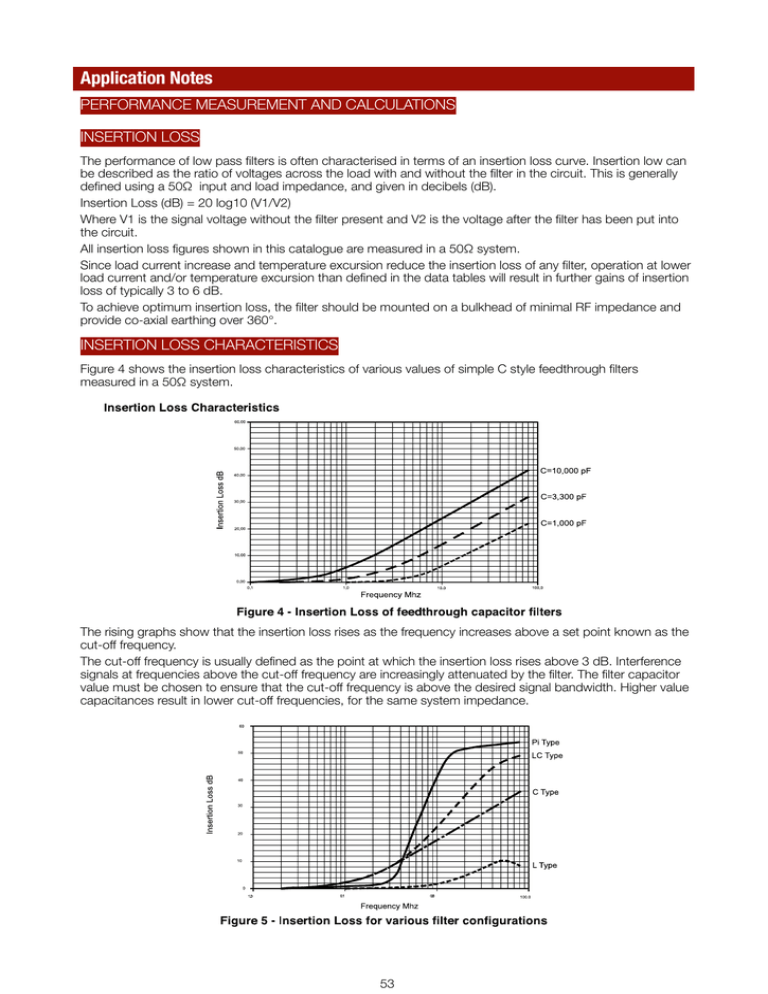
Application Notes PERFORMANCE MEASUREMENT AND CALCULATIONS INSERTION LOSS The performance of low pass filters is often characterised in terms of an insertion loss curve. Insertion low can be described as the ratio of voltages across the load with and without the filter in the circuit. This is generally defined using a 50Ω input and load impedance, and given in decibels (dB). Insertion Loss (dB) = 20 log10 (V1/V2) Where V1 is the signal voltage without the filter present and V2 is the voltage after the filter has been put into the circuit. All insertion loss figures shown in this catalogue are measured in a 50Ω system. Since load current increase and temperature excursion reduce the insertion loss of any filter, operation at lower load current and/or temperature excursion than defined in the data tables will result in further gains of insertion loss of typically 3 to 6 dB. To achieve optimum insertion loss, the filter should be mounted on a bulkhead of minimal RF impedance and provide co-axial earthing over 360°. INSERTION LOSS CHARACTERISTICS Figure 4 shows the insertion loss characteristics of various values of simple C style feedthrough filters measured in a 50Ω system. The rising graphs show that the insertion loss rises as the frequency increases above a set point known as the cut-off frequency. The cut-off frequency is usually defined as the point at which the insertion loss rises above 3 dB. Interference signals at frequencies above the cut-off frequency are increasingly attenuated by the filter. The filter capacitor value must be chosen to ensure that the cut-off frequency is above the desired signal bandwidth. Higher value capacitances result in lower cut-off frequencies, for the same system impedance. 53 Figure 5 shows a comparison of typical insertion loss characteristics of different filter configurations. These graphs show that although the insertion loss of an inductive element (L) on its own is very poor, when it is combined with a capacitor to form an LC filter the performance is improved dramatically. The inductive elements used in many leadthrough filters are in the form of a ferrite bead which has a drop off in attenuation at higher frequencies, leading to the flattening of the high frequency insertion loss response for the L and Pi types. The responsive curve of the Pi section filter shows an even steeper gradient beyond the cut-off frequency. In Figures 4 and 5 the characteristics are shown for the filters operating in a 50Ω system, however, the source and load impedance of the circuit in which the filter is operating can have a dramatic effect on the insertion loss. Figure 6 shows the relative low insertion loss of a C type filter operating with a 5Ω source instead of 50s. The graph also shows the dramatic improvement when the filter is replaced with an LC type. In this case the inductive element should be connected to the lower impedance side of the circuit. CURRENT The average line current must not exceed the rated current shown in the datasheet. At temperatures in excess of 105°C (221°F), up to a maximum of 125°C (257°F), the maximum current must be derated linearly to 0.6 times the rated current. The possibility of current transients or surges must be considered. The steady state line current plus the transient of surge current should not be allowed to exceed the following: • 1.5 times rated current for 10 secs • 4 times rated current for 500 ms • 8 times rated current for 50 ms In filter units incorporating inductors, an increase in line current will reduce the performance of the inductor and hence reduce the level of insertion loss achieved. The insertion loss claimed is only achieved within the load measurement condition defined. Devices specifying claiming insertion loss at full load current will exhibit higher insertion loss at lower currents. VOLTAGE The maximum voltage which may be applied to any filter element must not exceed the voltage rating of the device. The AC rated voltage is defined for operation up to 125°C (257°F) and for frequencies up to 400 Hz. The peak AC voltage must not exceed the defined DC voltage at 125°C (257°F). The possibility of voltage transients or spikes must be considered in determining the device voltage. TEMPERATURE The operating temperature for the device is defined in the specific voltage rating table - normally from -55°C (-67°F) to +85/+125°C (+185/+257°F). Temperature significantly affects the capacitor value and hence, the insertion loss achieved. The insertion loss claimed is only achieved within the temperature limits defined. The effect of line current in increasing the temperature of the filter must be remembered. Mounting onto a bulkhead, as well as providing an efficient RF screen, must also provide an efficient heat sink. The storage temperature of the device must not exceed the operating temperature limits. Extended storage at high ambient temperatures may cause degradation in the solderability of the terminations or discoloration of the finish. DC VOLTAGE DROP The effect of the resistance and rated current has been taken into consideration in the temperature rating of the filter. However, the voltage drop at line current should be borne in mind when selecting the current rating of the device. Higher current ratings should be selected if voltage drop must be minimised. 54

