EVB7107
315/433MHz Transmitter
Evaluation Board Description
Features
! Adjustable equivalent radiated power (ERP)
range from -25 dBm to -10 dBm
! Adjustable current consumption from
4.8 mA to 11.5 mA
! FSK deviation and center frequency
independently adjustable
! Differential output well-suited for loop antenna
! External clock available for µC drive,
down to 1.9 V supply
! ”Clock only” mode
! Conforms to EN 300 220 and similar standards
! Fully integrated, PLL-stabilized VCO
! Frequency range from 310 MHz to 440 MHz
! FSK through crystal pulling allows modulation
from DC to 40 kbit/s
! High FSK deviation possible for wideband data
transmission
! ASK achieved by on/off keying of internal
power amplifier
! FM possible with external varactor
! Wide power supply range from 2.2 V to 5.5 V
! High over-all frequency accuracy
! Very low standby current
Ordering Information
Part No.
EVB7107-433-FSK
EVB7107-315-FSK
EVB7107-433-ASK
EVB7107-315-ASK
Application Examples
!
!
!
!
!
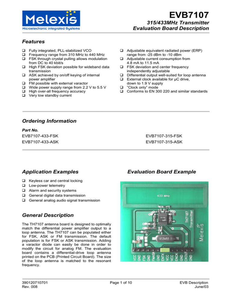
Evaluation Board Example
Keyless car and central locking
Low-power telemetry
Alarm and security systems
General digital data transmission
General analog audio signal transmission
General Description
The TH7107 antenna board is designed to optimally
match the differential power amplifier output to a
loop antenna. The TH7107 can be populated either
for FSK, ASK or FM transmission. The default
population is for FSK or ASK transmission. Adding
a varactor diode can easily be done in order to
modify the circuit for analog FM. The evaluation
board contains a differential-drive loop antenna
printed on the PCB (Printed Circuit Board). The size
of the loop antenna is matched to the resonant
frequency.
390120710701
Rev. 008
Page 1 of 10
EVB Description
June/03
EVB7107
315/433MHz Transmitter
Evaluation Board Description
Document Content
1
2
3
Theory of Operation ...................................................................................................3
1.1
General........................................................................................................................... 3
1.2
Block Diagram ................................................................................................................ 3
Functional Description ..............................................................................................4
2.1
FSK Modulation .............................................................................................................. 4
2.2
Frequency Modulation .................................................................................................... 4
2.3
ASK Modulation .............................................................................................................. 4
2.4
Mode Control Logic......................................................................................................... 4
Circuit Diagram ..........................................................................................................5
3.1
PCB Top View ................................................................................................................ 6
3.2
Board Connection ........................................................................................................... 6
3.3
Board Component Values ............................................................................................... 7
4
Package Information ..................................................................................................8
5
Disclaimer .................................................................................................................10
390120710701
Rev. 008
Page 2 of 10
EVB Description
June/03
EVB7107
315/433MHz Transmitter
Evaluation Board Description
1 Theory of Operation
1.1 General
As depicted in Fig.1, the TH71071 transmitter consists of a fully integrated voltage-controlled oscillator
(VCO), a divide-by-32 divider (div32), a phase-frequency detector (PFD) and a charge pump. An external
loop filter at pin LF determines the dynamic behaviour of the PLL and suppresses reference spurious signals.
The VCO’s output signal feeds the power amplifier (PA). RF signal power Po can be adjusted in six steps
from Po = –12 dBm to +2 dBm either by changing the value of resistor R1 or by varying the voltage VPS at pin
PS/DATA. The open-collector differential output (OUT1, OUT2) can be used to either directly drive a loop
antenna or to be converted to a single-ended impedance by means of a balanced-to-unbalanced (balun)
transformer. For maximum available output power, the differential output should be matched to a load of
about 1 kΩ.
Bandgap biasing ensures stable operation of the IC at a power supply range of 2.2 V to 5.5 V.
1.2 Block Diagram
RPS
VCC 10
VCC 15
PS
9
VEE
14
CKOUT
div 4
PA
div32
8
RO1
OUT2
12
PFD
5
XTAL
XOSC
mode
control
charge
pump
4
CX1
3
DATA
1
LF1
16 LF2
antenna
or
balun
VCC
VEE
11
VCO
RO2
CX2
OUT1
13
ENCK
7
ENTX
6
2 SUB
CF1
RF1
CF2
Fig. 1: Block diagram with external components
390120710701
Rev. 008
Page 3 of 10
EVB Description
June/03
EVB7107
315/433MHz Transmitter
Evaluation Board Description
2 Functional Description
2.1
FSK Modulation
A Colpitts crystal oscillator (XOSC) is used as the reference oscillator of a phase-locked loop (PLL)
synthesizer. FSK modulation is achieved by pulling the crystal (XTAL) through the data. So a CMOScompatible data stream applied at input DATA digitally modulates the XOSC. Two external pulling capacitors
CX1 and CX2 allow the FSK deviation and center frequency to be adjusted independently. At DATA = LOW
CX2 is connected in parallel to CX1 leading to the low-frequency component of the FSK spectrum (fmin);
while at DATA = HIGH CX2 is deactivated and the XOSC is set to its high frequency, leading to fmax.
An external reference signal can be directly AC-coupled to pin RO1. Then the TH7107 is used without an
XTAL. The reference signal has to contain the FSK (or FM) and sets the carrier frequency.
2.2
Frequency Modulation
For FM operation an external varactor is required. It simply acts as a pulling capacitor connected in series to
the crystal. Then the analog modulation signal, applied through a series resistor, directly modulates the
XOSC.
2.3
ASK Modulation
The TH7107 can be ASK-modulated by applying data directly at pin PS. This turns the PA on and off and
therefore leads to an ASK signal at the output.
2.4
Mode Control Logic
The mode control logic allows four different modes of operation as listed in the following table. The mode
control pins ENCK and ENTX are pulled-down internally. This guarantees that the whole circuit is shut down
if these pins are left floating.
The clock output CKOUT can be used to drive a µC. This output can be activated by the ENCK pin as
required for any specific application. Clock frequency is 1/4 of the reference crystal frequency.
ENCK
ENTX
Mode
Description
0
0
all OFF
whole circuit in standby
0
1
TX only
TX active, no clock available
1
0
clock only
TX standby and clock available
1
1
all ON
TX active and clock available
For more detailed information, please refer to the latest TH7107 data sheet revision.
390120710701
Rev. 008
Page 4 of 10
EVB Description
June/03
EVB7107
315/433MHz Transmitter
Evaluation Board Description
3 Circuit Diagram
C2
C1
RX
L1
C3
L2
C4
PS
CKOUT
XTAL
RF1
R3
CX3
CF2
8
ENCK
7
ENTX
6
RO1
4
5
RO2
DATA
3
SUB
2
1 LF1
RF2
CX2
9
10
VCC
VEE
OUT2
11
12
13
OUT1
14
VEE
15
VCC
LF2
16
RPS
CX1
CF1
V1
R1
R2
390120710701
Rev. 008
Page 5 of 10
1 2
CKOUT
GND
1 2 3
VCC
ENCK
GND
1 2
FM/ASK
GND
1 2
ENTX
VCC
1 2
FSK
GND
1 2
VCC
GND
C5
EVB Description
June/03
EVB7107
315/433MHz Transmitter
Evaluation Board Description
3.1
PCB Top View
Board layout data in Gerber format is available
433 MHZ
C2
C1
L2
L1
C4
RX
C3
RPS
RF2
16
9
1
R3
TH7107
8
CF2
CX1
Cx3
R1
V1
XTAL
R2
C5
GND
CKOUT
GND
ENCK
1
VCC
VCC
1
ENTX
GND
1
FM/ASK
GND
1
FSK
1
GND
1
VCC
Melexis
CX2
RF1
CF1
Board size is 48mm x 48mm
3.2
Board Connection
VCC
FSK
FM/ASK
CKOUT
Power supply (2.2 V to 5.5 V)
Input for FSK data (CMOS)
Input for FM signal (analog) or ASK data (CMOS)
Clock output (3.4 MHz)
390120710701
Rev. 008
ENCK
ENTX
GND
Page 6 of 10
Mode control pin (see para. 2.4))
Mode control pin (see para. 2.4))
Several ground pins
EVB Description
June/03
EVB7107
315/433MHz Transmitter
Evaluation Board Description
3.3
Board Component Values
Part
Size
Value
315 MHz
Value
433.6 MHz
Tolerance
CF1
0805
12 nF
10 nF
±10%
loop filter capacitor
CF2
0805
15 pF
12 pF
±10%
loop filter capacitor
XOSC capacitor for FSK (∆f = ±20 kHz)
XOSC capacitor for ASK, trimmed to fC
Description
CX1_FSK
0603
39 pF
39 pF
±5%
CX1_ASK
0603
68 pF
68 pF
±5%
CX2
0603
1 nF
1 nF
±5%
XOSC capacitor, only needed for FSK
CX3
0603
1 nF
1 nF
±10%
XOSC capacitor, only needed for FM
C1
1206
3.9 pF
3.9 pF
±2%
antenna resonance capacitor
C2
0805
3.9 pF
2.2 pF
±2%
antenna resonance capacitor
C3
0603
330 pF
330 pF
±10%
blocking capacitor
C4
0603
330 pF
330 pF
±10%
blocking capacitor
C5
1206
220 nF
220 nF
±20%
blocking capacitor
L1
0603
220 nH
220 nH
±10%
biasing inductor
L2
0603
220 nH
220 nH
±10%
biasing inductor
RF1
0805
2.0 kΩ
2.0 kΩ
±10%
loop filter resistor
RF2
0805
4.3 kΩ
4.3 kΩ
±10%
loop filter resistor
RPS
0805
56 kΩ
56 kΩ
±10%
power-select resistor, see data sheet para. 4.6
R1
0805
470 kΩ
470 kΩ
±10%
optional pull-up resistor, typically not needed
R2
0805
30 kΩ
30 kΩ
±10%
varactor bias resistor, only needed for FM
R3
0805
0Ω
0Ω
±10%
ASK jumper, only needed for ASK
RX
0603
damping resistor
V1
XTAL
SOD323
HC49/S
PCB
loop
antenna
PCB
loop
antenna
PCB
loop
antenna
4.7 kΩ
BB535
9.8438 MHz
fundamental
wave
4.7 kΩ
±10%
13.5500 MHz
fundamental
wave
±30ppm
calibration
±30ppm
temp.
long side
length
44 mm
44 mm
on FR4 PCB material
side length including length of C1 and C2
small side
length
20 mm
12 mm
on FR4 PCB material
Line width
2 mm
2 mm
on FR4 PCB material
varactor diode, only needed for FM
crystal, Cload = 12 pF to 15 pF, C0, max = 7 pF
Rm, max = 40 Ω
The listed component values are default values. All values might be changed to fit to any specific application.
As for example FSK deviation can be set by varying CX1 and CX2, output power at FSK/FM transmission
can be changed through RPS or through RPS and R3 at ASK transmission, respectively.
Pads for C1 are for population of a fixed-value capacitor with size 1206 or a to use trimming capacitor either.
390120710701
Rev. 008
Page 7 of 10
EVB Description
June/03
EVB7107
315/433MHz Transmitter
Evaluation Board Description
4 Package Information
D
ZD
e
7°
E
E1
16
1
0.254
(0.010)
L
DETAIL-A
b
7° + 3°
DETAIL-A
C
A1
A
A2
0.36 x 45°
BSC
(0.0014x45°)
.10 (.004)
Fig. 2: QSOP16 (Quarter size Small Outline Package)
all Dimension in mm, coplanarity < 0.1mm
min
max
D
E1
E
A
A1
A2
4.80
3.81
5.79
1.35
0.10
1.37
4.98
3.99
6.20
1.75
0.25
1.50
e
b
ZD
0.20
0.635
0.30
0.230
C
L
α
0.19
0.40
0°
0.25
1.27
8°
0.075
0.016
0°
0.098
0.050
8°
all Dimension in inch, coplanarity < 0.004”
min
max
0.189
0.196
390120710701
Rev. 008
0.150
0.157
0.228 0.0532 0.0040 0.054
0.244 0.0688 0.0098 0.059
0.008
0.025
Page 8 of 10
0.012
0.009
EVB Description
June/03
EVB7107
315/433MHz Transmitter
Evaluation Board Description
Your Notes
390120710701
Rev. 008
Page 9 of 10
EVB Description
June/03
EVB7107
315/433MHz Transmitter
Evaluation Board Description
5 Disclaimer
Devices sold by Melexis are covered by the warranty and patent indemnification provisions appearing in its
Term of Sale. Melexis makes no warranty, express, statutory, implied, or by description regarding the
information set forth herein or regarding the freedom of the described devices from patent infringement.
Melexis reserves the right to change specifications and prices at any time and without notice. Therefore, prior
to designing this product into a system, it is necessary to check with Melexis for current information. This
product is intended for use in normal commercial applications. Applications requiring extended temperature
range, unusual environmental requirements, or high reliability applications, such as military, medical lifesupport or life-sustaining equipment are specifically not recommended without additional processing by
Melexis for each application.
The information furnished by Melexis is believed to be correct and accurate. However, Melexis shall not be
liable to recipient or any third party for any damages, including but not limited to personal injury, property
damage, loss of profits, loss of use, interrupt of business or indirect, special incidental or consequential
damages, of any kind, in connection with or arising out of the furnishing, performance or use of the technical
data herein. No obligation or liability to recipient or any third party shall arise or flow out of Melexis’ rendering
of technical or other services.
© 2002 Melexis NV. All rights reserved.
For the latest version of this document. Go to our website at
www.melexis.com
Or for additional information contact Melexis Direct:
Europe and Japan:
All other locations:
Phone: +32 1367 0495
E-mail: sales_europe@melexis.com
Phone: +1 603 223 2362
E-mail: sales_usa@melexis.com
QS9000, VDA6.1 and ISO14001 Certified
390120710701
Rev. 008
Page 10 of 10
EVB Description
June/03
