MP2161
2A, 6V, 1.5MHz, 17μA IQ, COT
Synchronous Step Down Switcher
In 8-pin TSOT23
The Future of Analog IC Technology
DESCRIPTION
FEATURES
The MP2161 is a monolithic step-down switch
mode converter with built-in internal power
MOSFETs. It achieves 2A continuous output
current from a 2.5V to 6V input voltage with
excellent load and line regulation. The output
voltage can be regulated as low as 0.6V.
•
•
•
•
The
Constant-On-Time
control
scheme
provides fast transient response and eases loop
stabilization. Fault condition protection includes
cycle-by-cycle current limiting and thermal
shutdown.
The MP2161 is available in the small TSOT23-8
package and requires a minimum number of
readily available standard external components.
The MP2161 is ideal for a wide range of
applications including High Performance DSPs,
FPGAs, PDAs, and portable instruments.
•
•
•
•
•
•
•
Very Low IQ: 17μA
Default 1.5MHz Switching Frequency
EN and Power Good for Power Sequencing
Wide 2.5V to 6V Operating Input Range
Output Adjustable from 0.6V
Up to 2A Output Current
100% Duty Cycle in Dropout
100mΩ and 60mΩ Internal Power MOSFET
Switches
Cycle-by-Cycle Over Current Protection
Short Circuit Protect with Hiccup Mode
Stable with Low ESR Output Ceramic
Capacitors
Available in a TSOT23-8 Package
APPLICATIONS
•
•
•
•
Wireless/Networking Cards
Portable Instruments
Battery Powered Devices
Low Voltage I/O System Power
All MPS parts are lead-free and adhere to the RoHS directive. For MPS green
status, please visit MPS website under Products, Quality Assurance page.
“MPS” and “The Future of Analog IC Technology” are registered trademarks of
Monolithic Power Systems, Inc.
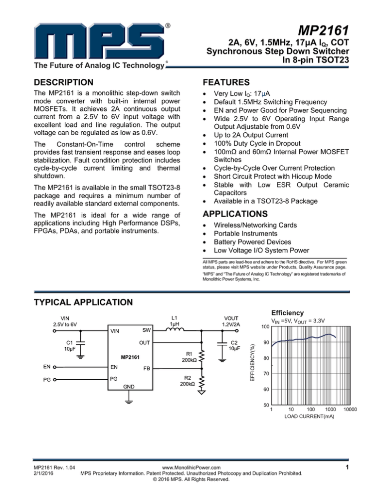
TYPICAL APPLICATION
MP2161 Rev. 1.04
2/1/2016
www.MonolihicPower.com
MPS Proprietary Information. Patent Protected. Unauthorized Photocopy and Duplication Prohibited.
© 2016 MPS. All Rights Reserved.
1
MP2161 – 2A, 6V, 1.5MHz SYNCHRONOUS STEP-DOWN SWITCHER
ORDERING INFORMATION
Part Number*
MP2161GJ
Package
TSOT23-8
Top Marking
AEB
* For Tape & Reel, add suffix –Z (e.g. MP2161GJ–Z);
PACKAGE REFERENCE
TOP VIEW
PG
1
8
EN
VIN
2
7
FB
SW
3
6
AGND
PGND
4
5
OUT
TSOT23-8
ABSOLUTE MAXIMUM RATINGS (1)
Thermal Resistance
Supply Voltage VIN ...................................... 6.5V
VSW ......................................................................
-0.3V (-1.5V for <10ns) to 6.5V (7V for <10ns)
All Other Pins ................................-0.3V to 6.5 V
Junction Temperature ...............................150°C
Lead Temperature ....................................260°C
(2)
Continuous Power Dissipation (TA = +25°C)
……….….. ............................................... 1.25W
Storage Temperature............... -65°C to +150°C
TSOT23-8.............................. 100 ..... 55... °C/W
Recommended Operating Conditions
(3)
Supply Voltage VIN .............................2.5V to 6V
Operating Junction Temp. (TJ). -40°C to +125°C
MP2161 Rev. 1.04
2/1/2016
(4)
θJA
θJC
Notes:
1) Exceeding these ratings may damage the device.
2) The maximum allowable power dissipation is a function of the
maximum junction temperature TJ (MAX), the junction-toambient thermal resistance θJA, and the ambient temperature
TA. The maximum allowable continuous power dissipation at
any ambient temperature is calculated by PD (MAX) = (TJ
(MAX)-TA)/θJA. Exceeding the maximum allowable power
dissipation will cause excessive die temperature, and the
regulator will go into thermal shutdown. Internal thermal
shutdown circuitry protects the device from permanent
damage.
3) The device is not guaranteed to function outside of its
operating conditions.
4) Measured on JESD51-7, 4-layer PCB.
www.MonolihicPower.com
MPS Proprietary Information. Patent Protected. Unauthorized Photocopy and Duplication Prohibited.
© 2016 MPS. All Rights Reserved.
2
MP2161 – 2A, 6V, 1.5MHz SYNCHRONOUS STEP-DOWN SWITCHER
ELECTRICAL CHARACTERISTICS (5)
VIN = 5V, TA = +25°C, unless otherwise noted.
Parameter
Symbol
Feedback Voltage
VFB
Feedback Current
PFET Switch On Resistance
NFET Switch On Resistance
IFB
Condition
2.5V ≤ VIN ≤ 6V
o
o
TA=-40 C to +85 C
(6)
Min
Typ
Max
-3%
0.600
+3%
-3.5%
VFB = 0.6V
RDSON_P
RDSON_N
VEN = 0V, VIN = 6V
VSW = 0V and 6V
Switch Leakage
PFET Current Limit
2.7
ON Time
TON
Switching frequency
Minimum Off Time
Soft-Start Time
Fs
-20%
-25%
TMIN-OFF
TSS-ON
Power Good Upper Trip Threshold
PGH
Power Good Lower Trip Threshold
Power Good Delay
Power Good Sink Current
Capability
Power Good Logic High Voltage
Power Good Internal Pull Up
Resistor
Under Voltage Lockout Threshold
Rising
Under Voltage Lockout Threshold
Hysteresis
EN Input Logic Low Voltage
EN Input Logic High Voltage
PGL
PGD
EN Input Current
Supply Current (Shutdown)
Supply Current (Quiescent)
Thermal Shutdown(5)
Thermal Hysteresis
VIN=5V, VOUT=1.2V
VIN=3.6V, VOUT=1.2V
VOUT=1.2V
TA=-40oC to +85oC(6)
(5)
FB voltage respect to the
regulation
VPG-L
Sink 1mA
VPG-H
VIN=5V, VFB=0.6V
+3.5%
50
nA
mΩ
mΩ
0
1
μA
3.2
185
245
1500
1500
60
1.5
4.0
A
ns
+20%
+25%
%
-10
50
%
μs
V
V
550
2.3
kΩ
2.45
260
1.2
1.5
0
20
17
V
mV
0.4
VEN=2V
VEN=0V
VEN=0V, VIN=3V
VEN=2V, VFB=0.63V, VIN=5V
kHz/%
kHz/%
ns
ms
+10
4.9
2.15
V/%
10
100
60
0.4
RPG
Units
100
20
V
V
μA
μA
nA
μA
150
°C
30
°C
Notes:
5) Guaranteed by design.
6) Guaranteed by characterization test.
MP2161 Rev. 1.04
2/1/2016
www.MonolihicPower.com
MPS Proprietary Information. Patent Protected. Unauthorized Photocopy and Duplication Prohibited.
© 2016 MPS. All Rights Reserved.
3
MP2161 – 2A, 6V, 1.5MHz SYNCHRONOUS STEP-DOWN SWITCHER
TYPICAL PERFORMANCE CHARACTERISTICS
VIN = 5V, VOUT = 1.2V, L = 1.0µH, TA = +25ºC, unless otherwise noted.
Quiescent Current vs.
Input Voltage
Shutdown Current vs.
Input Voltage
40
Load Regulation
2.00
0.003
1.50
0.0025
VIN=5V
1.00
30
20
0.002
0.50
0.0015
0.00
-0.50
0.001
VIN=6V
-1.00
10
0.0005
-1.50
0
0
2
2.5
3
3.5
4
4.5 5
-2.00
2
5.5 6
2.5 3
3.5
4 4.5
5 5.5
6
0
INPUT VOLTAGE (V)
INPUT VOLTAGE (V)
Line Regulation
50
45
40
40
35
35
0.20
30
30
0.00
25
25
-0.20
20
20
15
15
-0.60
10
10
-0.80
5
0
5
0
0.40
Load=1A
-0.40
-1.00
Load=2A
Load=0A
2
3
4
5
6
0
INPUT VOLTAGE (V)
1
1.5
2
0
2.5
Efficiency
100
2.5
0.5
1
1.5
2
2.5
OUTPUT CURRENT (A)
OUTPUT CURRENT (A)
Efficiency
100
95
90
0.5
2
VIN=5V, VOUT=3.3V
50
45
0.60
1.5
Case Temp Rise
Case Temp Rise
0.80
1
LOAD CURRENT (A)
VIN=3V, VOUT=1.2V
1.00
0.5
Efficiency
5/3.3VIN to 1.8VOUT
5VIN to 3.3VOUT
100
VIN=3.3V
90
90
85
80
80
75
VIN=6V
VIN=5V
70
VIN=5V
80
VIN=3.3V
70
70
60
60
65
60
55
50
1
10
100
1000 10000
LOAD CURRENT(mA)
MP2161 Rev. 1.04
2/1/2016
50
0
0.5
1
1.5
IOUT (A)
2
2.5
50
0
0.5
1
1.5
IOUT (A)
www.MonolihicPower.com
MPS Proprietary Information. Patent Protected. Unauthorized Photocopy and Duplication Prohibited.
© 2016 MPS. All Rights Reserved.
2
2.5
4
MP2161 – 2A, 6V, 1.5MHz SYNCHRONOUS STEP-DOWN SWITCHER
TYPICAL PERFORMANCE CHARACTERISTICS (continued)
VIN = 5V, VOUT = 1.2V, L = 1.0µH, TA = +25ºC, unless otherwise noted.
MP2161 Rev. 1.04
2/1/2016
www.MonolihicPower.com
MPS Proprietary Information. Patent Protected. Unauthorized Photocopy and Duplication Prohibited.
© 2016 MPS. All Rights Reserved.
5
MP2161 – 2A, 6V, 1.5MHz SYNCHRONOUS STEP-DOWN SWITCHER
TYPICAL PERFORMANCE CHARACTERISTICS (continued)
VIN = 5V, VOUT = 1.2V, L = 1.0µH, TA = +25ºC, unless otherwise noted
MP2161 Rev. 1.04
2/1/2016
www.MonolihicPower.com
MPS Proprietary Information. Patent Protected. Unauthorized Photocopy and Duplication Prohibited.
© 2016 MPS. All Rights Reserved.
6
MP2161 – 2A, 6V, 1.5MHz SYNCHRONOUS STEP-DOWN SWITCHER
PIN FUNCTIONS
Pin #
1
2
3
4
5
6
7
8
MP2161 Rev. 1.04
2/1/2016
Name
Description
Power Good Indicator. The output of this pin is an open drain with internal pull up resistor
PG
to VIN. PGOOD is pulled up to VIN when the FB voltage is within 10% of the regulation
level, if FB voltage is out of that regulation range, it is LOW.
Supply Voltage. The MP2161 operates from a +2.5V to +6V unregulated input. C1 is
VIN
needed to prevent large voltage spikes from appearing at the input.
SW
Switch Output
PGND Power ground
OUT Input sense pin for output voltage
AGND Analogy ground for internal control circuit
Feedback pin. An external resistor divider from the output to GND, tapped to the FB pin,
FB
sets the output voltage.
EN
On/Off Control
www.MonolihicPower.com
MPS Proprietary Information. Patent Protected. Unauthorized Photocopy and Duplication Prohibited.
© 2016 MPS. All Rights Reserved.
7
MP2161 – 2A, 6V, 1.5MHz SYNCHRONOUS STEP-DOWN SWITCHER
BLOCK DIAGRAM
VIN
Bias
&
Voltage
Reference
EN
Soft start
+
COMP
VTH
Lo-Iq
0.6V
RST
+
+ E.A.
-
Constant
On -Time
Pulse
PDRV
PWM
Main
Switch
(PCH)
PWM
+
Lo-Iq
+
FB
SW
EN
FBCOMP
Driver
VOUT
Lo-Iq
Ramp
Generator
Synchronous
Rectifier
( NCH)
SW
Lo-Iq
Hi-Z
NDRV
OUT
GND
VIN
FB for
Fixed Output
0.66V
+
+
COMP
COMP
-
Lo-Iq
+
COMP
0.54V
PG
-
Figure 1: MP2161 Block Diagram
MP2161 Rev. 1.04
2/1/2016
www.MonolihicPower.com
MPS Proprietary Information. Patent Protected. Unauthorized Photocopy and Duplication Prohibited.
© 2016 MPS. All Rights Reserved.
8
MP2161 – 2A, 6V, 1.5MHz SYNCHRONOUS STEP-DOWN SWITCHER
OPERATION
MP2161 uses constant on-time control with
input voltage feed forward to stabilize the
switching frequency over full input range. At
light load, MP2161 employs a proprietary
control of low side switch and inductor current
to eliminate ringing on switching node and
improve efficiency.
Constant On-time Control
Compare to fixed frequency PWM control,
constant on-time control offers the advantage of
simpler control loop and faster transient response.
By using input voltage feed forward, MP2161
maintains a nearly constant switching frequency
across input and output voltage range. The ontime of the switching pulse can be estimated as:
TON =
VOUT
⋅ 0.667μs
VIN
To prevent inductor current run away during load
transient, MP2161 fixes the minimum off time to
be 60ns. However, this minimum off time limit will
not affect operation of MP2161 in steady state in
any way.
Light Load Operation
In light load condition, MP2161 uses a
proprietary control scheme to save power and
improve efficiency. The MP2161 will turn off the
low side switch when inductor current starts to
reverse. Then MP2161 works in discontinuous
conduction mode (DCM) operation.
The DCM mode happens only after low side
switch turned off by ZCD circuit. Considering
the ZCD circuit propagation time, the typical
delay is 30ns. It means the inductor current still
fall after the ZCD is trigger during this delay. If
the inductor current falling slew rate is fast (Vo
voltage is high or close to Vin), the low side
MOSFET is turned off at the moment inductor
current may be negative. This phenomena will
cause MP2161 can not enter DCM operation. If
the DCM mode is required, the off time of low
side MOSFET in CCM should be longer than
60ns. It means the maximum duty is 90% to
guarantee DCM mode at light load.
For example, VIN is 3.4V and VOUT is 3.3V, the
off time in CCM is 20ns. It is difficult to enter
MP2161 Rev. 1.04
2/1/2016
DCM at light load. And using smaller inductor
can improve it and make it enter DCM easily.
Enable
When input voltage is greater than the undervoltage lockout threshold (UVLO), typically 2.3V,
MP2161 can be enabled by pulling EN pin to
higher than 1.2V. Leaving EN pin float or pull
down to ground will disable MP2161. There is
an internal 1Meg Ohm resistor from EN pin to
ground.
Soft Start
MP2161 has built-in soft start that ramps up the
output voltage in a controlled slew rate,
avoiding overshoot at startup. The soft start
time is about 1.5ms typical.
Power GOOD Indictor
MP2161 has an open drain with 550kΩ pull-up
resistor pin for power good indicator PGOOD.
When FB pin is within +/-10% of regulation
voltage, i.e. 0.6V, PGOOD pin is pulled up to
VIN by the internal resistor. If FB pin voltage is
out of the +/-10% window, PGOOD pin is pulled
down to ground by an internal MOS FET. The
MOS FET has a maximum Rdson of less than
100 Ohm.
Current limit
MP2161 has a typical 3.2A current limit for the
high side switch. When the high side switch hits
current limit, MP2161 will touch the hiccup
threshold until the current lower down. This will
prevent inductor current from continuing to build
up which will result in damage of the
components.
Short Circuit and Recovery
MP2161 enters short circuit protection mode
also when the current limit is hit, and tries to
recover from short circuit with hiccup mode. In
short circuit protection, MP2161 will disable
output power stage, discharge soft-start cap
and then automatically try to soft-start again. If
the short circuit condition still holds after softstart ends, MP2161 repeats this operation cycle
till short circuit disappears and output rises
back to regulation level.
www.MonolihicPower.com
MPS Proprietary Information. Patent Protected. Unauthorized Photocopy and Duplication Prohibited.
© 2016 MPS. All Rights Reserved.
9
MP2161 – 2A, 6V, 1.5MHz SYNCHRONOUS STEP-DOWN SWITCHER
APPLICATION INFORMATION
COMPONENT SELECTION
Setting the Output Voltage
The external resistor divider is used to set the
output voltage (see Typical Application on page
1). The feedback resistor R1 can not be too
large neither too small considering the trade-off
for stability and dynamic. Choose R1 to be
around 120kΩ to 200kΩ. R2 is then given by:
R2 =
R1
Vout
−1
0.6
The feedback circuit is shown as Figure 2.
Vout
MP2161
R1
FB
Figure 2: Feedback Network
Table 1 lists the recommended resistors value
for common output voltages.
Table 1—Resistor Selection for Common
Output Voltages
R1 (kΩ)
200(1%)
200(1%)
200(1%)
200(1%)
200(1%)
R2 (kΩ)
300(1%)
200(1%)
100(1%)
63.2(1%)
44.2(1%)
Selecting the Inductor
A 0.68µH to 2.2µH inductor is recommended for
most applications. For highest efficiency, the
inductor DC resistance should be less than
15mΩ. For most designs, the inductance value
can be derived from the following equation.
L1 =
VOUT × (VIN − VOUT )
VIN × ΔIL × fOSC
Where ΔIL is the inductor ripple current.
MP2161 Rev. 1.04
2/1/2016
IL(MAX) = ILOAD +
ΔI L
2
Selecting the Input Capacitor
The input current to the step-down converter is
discontinuous, therefore a capacitor is required to
supply the AC current to the step-down converter
while maintaining the DC input voltage. Use low
ESR capacitors for the best performance. Ceramic
capacitors with X5R or X7R dielectrics are
highly recommended because of their low ESR
and small temperature coefficients. For most
applications, a 10µF capacitor is sufficient. For
higher output voltage, 47uF may be needed for
more stable system.
Since the input capacitor absorbs the input
switching current it requires an adequate ripple
current rating. The RMS current in the input
capacitor can be estimated by:
R2
VOUT (V)
1.0
1.2
1.8
2.5
3.3
Choose inductor current to be approximately
30% of the maximum load current. The
maximum inductor peak current is:
I C1 = ILOAD ×
VOUT ⎛⎜ VOUT
× 1−
VIN
VIN ⎜⎝
⎞
⎟
⎟
⎠
The worse case condition occurs at VIN = 2VOUT,
where:
IC1 =
ILOAD
2
For simplification, choose the input capacitor
whose RMS current rating greater than half of
the maximum load current.
The input capacitor can be electrolytic, tantalum
or ceramic. When using electrolytic or tantalum
capacitors, a small and high quality ceramic
capacitor, i.e. 0.1μF, should be placed as close
to the IC as possible. When using ceramic
capacitors, make sure that they have enough
capacitance to provide sufficient charge to
prevent excessive voltage ripple at input. The
input voltage ripple caused by capacitance can
be estimated by:
ΔVIN =
⎛
ILOAD
V
V ⎞
× OUT × ⎜ 1 − OUT ⎟
fS × C1 VIN ⎝
VIN ⎠
www.MonolihicPower.com
MPS Proprietary Information. Patent Protected. Unauthorized Photocopy and Duplication Prohibited.
© 2016 MPS. All Rights Reserved.
10
MP2161 – 2A, 6V, 1.5MHz SYNCHRONOUS STEP-DOWN SWITCHER
Selecting the Output Capacitor
The output capacitor (C2) is required to
maintain the DC output voltage. Ceramic
capacitors are recommended. Low ESR
capacitors are preferred to keep the output
voltage ripple low. The output voltage ripple can
be estimated by:
ΔVOUT =
⎞
VOUT ⎛ VOUT ⎞ ⎛
1
× ⎜1 −
⎟
⎟ × ⎜ RESR +
fS × L1 ⎝
VIN ⎠ ⎝
8 × fS × C2 ⎠
Where L1 is the inductor value and RESR is the
equivalent series resistance (ESR) value of the
output capacitor.
Using ceramic capacitors, the impedance at the
switching frequency is dominated by the
capacitance. The output voltage ripple is mainly
caused by the capacitance. For simplification,
the output voltage ripple can be estimated by:
Proper layout of the switching power supplies is
very important, and sometimes critical for
proper function. For the high-frequency
switching converter, poor layout design can
result in poor line or load regulation and stability
issues.
The high current paths (GND, IN and SW)
should be placed very close to the device with
short, direct and wide traces. The input
capacitor needs to be as close as possible to
the IN and GND pins. The external feedback
resistors should be placed next to the FB pin.
Keep the switching node SW short and away
from the feedback network.
PG
AGND
⎛ V ⎞
VOUT
× ⎜ 1 − OUT ⎟
2
VIN ⎠
8 × fS × L1 × C2 ⎝
C1
In the case of tantalum or electrolytic capacitors,
the ESR dominates the impedance at the
switching frequency. For simplification, the
output ripple can be approximated to:
ΔVOUT =
VOUT ⎛
V
⎞
× ⎜ 1 − OUT ⎟ × RESR
fS × L1 ⎝
VIN ⎠
The characteristics of the output capacitor also
affect the stability of the regulation system.
EN
1
2
3
4
8
7
6
5
R2
R1
ΔVOUT =
PCB Layout
C2
SW
VIN
GND
OUT
Figure 3: PCB Layout Recommendation
Design Example
Below is a design example following the
application guidelines for the specifications:
Table 2: Design Example
5V
VIN
1.2V
VOUT
1500kHz
fSW
The detailed application schematic is shown in
Figure 4. The typical performance and circuit
waveforms have been shown in the Typical
Performance Characteristics section. For more
device applications, please refer to the related
Evaluation Board Datasheets.
MP2161 Rev. 1.04
2/1/2016
www.MonolihicPower.com
MPS Proprietary Information. Patent Protected. Unauthorized Photocopy and Duplication Prohibited.
© 2016 MPS. All Rights Reserved.
11
MP2161 – 2A, 6V, 1.5MHz SYNCHRONOUS STEP-DOWN SWITCHER
TYPICAL APPLICATION CIRCUITS
Figure 4: Typical Application Circuit
MP2161 Rev. 1.04
2/1/2016
www.MonolihicPower.com
MPS Proprietary Information. Patent Protected. Unauthorized Photocopy and Duplication Prohibited.
© 2016 MPS. All Rights Reserved.
12
MP2161 – 2A, 6V, 1.5MHz SYNCHRONOUS STEP-DOWN SWITCHER
PACKAGE INFORMATION
TSOT23-8
See note 7
EXAMPLE
TOP MARK
PIN 1 ID
IAAAA
RECOMMENDED LAND PATTERN
TOP VIEW
SEATING PLANE
SEE DETAIL''A''
FRONT VIEW
SIDE VIEW
NOTE:
DETAIL ''A''
1) ALL DIMENSIONS ARE IN MILLIMETERS
.
2) PACKAGE LENGTH DOES NOT INCLUDE MOLD FLASH
,
PROTRUSION OR GATE BURR.
3) PACKAGE WIDTH DOES NOT INCLUDE INTERLEAD
FLASH OR PROTRUSION.
4) LEAD COPLANARITY(BOTTOM OF LEADS AFTER
FORMING) SHALL BE 0.10 MILLIMETERS MAX.
5) JEDEC REFERENCE IS MO-193, VARIATION BA.
6) DRAWING IS NOT TO SCALE.
7) PIN 1 IS LOWER LEFT PIN WHEN READING TOP MARK
FROM LEFT TO RIGHT, (SEE EXAMPLE TOP MARK)
NOTICE: The information in this document is subject to change without notice. Please contact MPS for current specifications.
Users should warrant and guarantee that third party Intellectual Property rights are not infringed upon when integrating MPS
products into any application. MPS will not assume any legal responsibility for any said applications.
MP2161 Rev. 1.04
2/1/2016
www.MonolithicPower.com
MPS Proprietary Information. Patent Protected. Unauthorized Photocopy and Duplication Prohibited.
© 2016 MPS. All Rights Reserved.
13
