Product Specification
PE42920
UltraCMOS® Passive DDSPDT
High-Isolation RF Switch
10 kHz–6 GHz
Product Description
The PE42920 is a dual differential single pole double
throw (DDSPDT) RF switch developed on Peregrine’s
UltraCMOS® process technology. It is a broadband and
low loss device enabling the switching of two
independent differential signals. This device consumes
less power than active differential switches and offers 2
kV HBM ESD protection. It has high isolation between
same channel inputs as well as opposite active channels.
It has been designed for low phase mismatch between
matched paths.
Features
Dual differential single pole double
The PE42920 is manufactured on Peregrine’s
UltraCMOS process, a patented variation of silicon-oninsulator (SOI) technology on a sapphire substrate,
offering the performance of GaAs with the economy and
integration of conventional CMOS.
throw switch
Broadband: 10 kHz to 6 GHz
Low frequency insertion loss: 0.7 dB
typical
High isolation between same channels
at 6 GHz: 26 dB typical
High isolation between opposite active
channels at 6 GHz: 30 dB typical
Low phase mismatch between matched
paths at 6 GHz: 15 degrees typical
High ESD performance: 2 kV HBM
Figure 2. Package Type
16-lead 3 × 3 mm QFN
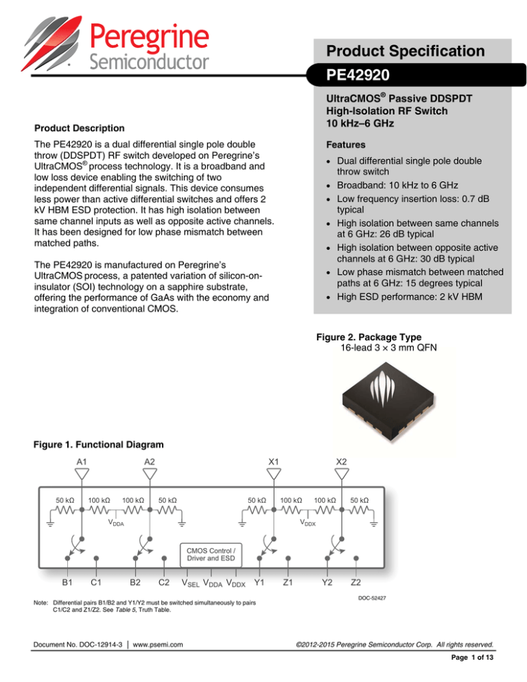
Figure 1. Functional Diagram
A1
50 kΩ
A2
100 kΩ
100 kΩ
X1
50 kΩ
50 kΩ
X2
100 kΩ
VDDA
100 kΩ
50 kΩ
VDDX
CMOS Control /
Driver and ESD
B1
C1
B2
C2
VSEL VDDA VDDX
Y1
Note: Differential pairs B1/B2 and Y1/Y2 must be switched simultaneously to pairs
C1/C2 and Z1/Z2. See Table 5, Truth Table.
Document No. DOC-12914-3 │ www.psemi.com
Z1
Y2
Z2
DOC-52427
©2012-2015 Peregrine Semiconductor Corp. All rights reserved.
Page 1 of 13
PE42920
Product Specification
Table 1. Typical Specifications VDD = 3.3V, Temp = +25 °C (ZS = ZL = 100Ω differential)
Min/Max Specifications VDD = 3.3V ±10%, –40 °C ≤ Temp ≤ +85 °C, (ZS = ZL = 100Ω differential)
AC coupled – external DC blocking caps
Electrical Parameter
Operating frequency
Condition/Notes
Min
Frequency range
Typ
10 kHz
Differential 3 dB bandwidth
5.6
Max
Unit
6 GHz
As shown
6
GHz
Insertion loss at 10 kHz
VCM = 1.1V
0.7
1.25
dB
Insertion loss at 1 GHz
VCM = 1.1V
1.0
1.4
dB
Isolation between same
channel inputs at 6 GHz
A to C when B is ON. A to B when C is ON
X to Z when Y ON. X to Y when Z is ON
24
26
dB
Isolation between opposite
(active) channels at 6 GHz
Channels A ↔ X. VCM = 1.1V
25
30
dB
Input 1dB compression* (P1dB)
VCM = 1.1V, differential
10
13
dBm
Differential
50–1250 MHz
1250–2500 MHz
2500–4000 MHz
12.5
8
5.5
14
9
8
dB
dB
dB
Single ended
50–1250 MHz
1250–2500 MHz
2500–4000 MHz
14.5
12
10.5
17.5
14
13
dB
dB
Differential
50–1250 MHz
1250–2500 MHz
2500–4000 MHz
12.5
8.5
8
15.5
9.5
9.5
dB
dB
dB
Single ended
50–1250 MHz
1250–2500 MHz
2500–4000 MHz
16
13
10.5
18.5
16
14.5
dB
dB
dB
Return loss
common ports A and X
Return loss
active ports B, C, Y, Z
Switching time
50% control to 10/90% RF
Phase mismatch on matched
paths at 6 GHz
VSEL = 1 matched paths
(A1 ↔ B1 & A2 ↔ B2)
(X1 ↔ Y1 & X2 ↔ Y2)
Phase mismatch on
un-matched paths at 6 GHz
Unmatched: average of A1,A2 delay to average of X1,X2
Phase delta stability
Across voltage and temperature
Common mode voltage
Common port self biased VCM (Vcm ≈ VDD/3)
Common mode impedance
Common port bias
resistances
Input IP3
Single ended (see Figure 19)
VSEL = 0 matched paths
(A1 ↔ C1 & A2 ↔ C2)
(X1 ↔ Z1 & X2 ↔ Z2)
ZCM to VDD
ZCM to GND
270
450
ns
VCM = 1.1V
15
30
degrees
VCM = 1.1V
22
50
degrees
2
degrees
1.1
V
100
50
kΩ
kΩ
dBm
Note: * P1dB is an indication of device linearity, max operating power is restricted to limits in Table 3.
©2012-2015 Peregrine Semiconductor Corp. All rights reserved.
Page 2 of 13
Document No. DOC-12914-3 │ UltraCMOS® RFIC Solutions
PE42920
Product Specification
Table 3. Operating Ranges2
Figure 3. Pin Configuration (Top View)
Y2
VDD1 Power Supply Voltage
Min
Typ
Max
2.97
3.3
3.63
V
100
500
µA
85
°C
2
mW
IDD Supply Current
13
Y1
14
15
Z1
16
Z2
Parameter
Pin 1 Dot
Marking
TOP Operating Temperature
–40
PDC DC Power Consumption
C2
1
C1
2
B2
3
VDDX
11
10
VIH VSEL Control Voltage High
0.7xVDD
VDD
V
X2
VIL VSEL Control Voltage Low
0
0.3xVDD
V
X1
IIH/IIL ISEL Control Current –
Input High/Low
1
µA
PMAX Max. Input Power
(100Ω Differential, Active Port)
10
dBm
PMAX Max. Input Power
(50Ω Single Ended, Active Port)
7
dBm
2.8
1.4
VPP
VPP
8
VSEL
GND
A2
A1
VDDA
7
9
6
4
5
B1
Exposed
Ground Pad
12
Unit
Table 2. Pin Descriptions
Description
VPEAK-TO-PEAK Max Input
Differential (100Ω)
Single Ended (50Ω)
Notes: 1. Operating below min. VDD results in degraded performance.
2. Operation should be restricted to the limits in the Operating Ranges
table.
Table 4. Absolute Maximum Ratings
Pin No.
Pin Name
1
C2
C-channel [Logic Low] RF Port –
Parameter/Condition
2
C1
C-channel [Logic Low] RF Port +
3
B2
B-channel [Logic High] RF Port –
4
B1
B-channel [Logic High] RF Port +
5
VDDA
6
Max
Unit
PMAX Max. Input Power
(100Ω Differential, Active Port)
10
dBm
PMAX Max. Input Power
(50Ω Single Ended, Active Port)
7
dBm
A-channel Supply
VSEL Control Voltage
4
V
A1
A-channel RF Common Port +
ISW DC Current on RF Path
5
mA
7
A2
A-channel RF Common Port –
TST Storage Temperature
+150
°C
8
GND
Ground
2000
V
9
VSEL
Simultaneous Logic Select
VESD MM ESD Voltage
100
V
10
X1
X-channel RF Common Port +
11
X2
X-channel RF Common Port –
VPEAK-TO-PEAK Max Input
Differential (100Ω)
Single Ended (50Ω)
2.8
1.4
VPP
VPP
12
VDDX
13
Y2
Y-channel [Logic High] RF Port –
14
Y1
Y-channel [Logic High] RF Port +
15
Z2
Z-channel [Logic Low] RF Port –
16
Z1
Z-channel [Logic Low] RF Port +
Paddle
GND
Exposed solder pad: Ground for
proper operation
Document No. DOC-12914-3
X-channel Supply
│ www.psemi.com
VESD HBM ESD Voltage
1
2
Min
–65
Notes: 1. HBM ESD Voltage (HBM, MIL_STD 883, Method 3015.7).
2. MM ESD Voltage (JESD22-A115-A).
Exceeding absolute maximum ratings may cause
permanent damage. Operation between operating
range maximum and absolute maximum for
extended periods may reduce reliability.
©2012-2015 Peregrine Semiconductor Corp. All rights reserved.
Page 3 of 13
PE42920
Product Specification
Electrostatic Discharge (ESD) Precautions
When handling this UltraCMOS device, observe
the same precautions that you would use with
other ESD-sensitive devices. Although this device
contains circuitry to protect it from damage due to
ESD, precautions should be taken to avoid
exceeding the specified rating.
Table 5. Truth Table: Signal-Path Control Logic
Path
Channel A
Channel X
VSEL
AB
AC
XY
XZ
Low
OFF
ON
OFF
ON
High
ON
OFF
ON
OFF
A = Differential pair A1/A2
C = Differential pair C1/C2
Y = Differential pair Y1/Y2
B = Differential pair B1/B2
X = Differential pair X1/X2
Z = Differential pair Z1/Z2
Latch-Up Avoidance
Unlike conventional CMOS devices, UltraCMOS
devices are immune to latch-up.
Moisture Sensitivity Level
The Moisture Sensitivity Level rating for the
PE42920 in the 16-lead 3 × 3 mm QFN package is
MSL1.
©2012-2015 Peregrine Semiconductor Corp. All rights reserved.
Page 4 of 13
Document No. DOC-12914-3 │ UltraCMOS® RFIC Solutions
PE42920
Product Specification
Typical Performance Data @ 3.3V and +25 °C, unless otherwise specified
Figure 4. Differential Insertion Loss over VDD
Figure 5. Differential Insertion Loss over Temp
Figure 6. Differential Active Port (B, C, Y, or Z)
Return Loss over VDD
Figure 7. Differential Active Port (B, C, Y, or Z)
Return Loss over Temp
Document No. DOC-12914-3
│ www.psemi.com
©2012-2015 Peregrine Semiconductor Corp. All rights reserved.
Page 5 of 13
PE42920
Product Specification
Typical Performance Data @ 3.3V and +25 °C, unless otherwise specified
Figure 8. Differential Common Port (A or X)
Return Loss over VDD
Figure 9. Differential Common Port (A or X)
Return Loss over Temp
Figure 10. Single-Ended Active Port
(B1, B2, C1, C2, Y1, Y2)
Return Loss over VDD
Figure 11. Single-Ended Active Port
(B1, B2, C1, C2, Y1, Y2)
Return Loss over Temp
©2012-2015 Peregrine Semiconductor Corp. All rights reserved.
Page 6 of 13
Document No. DOC-12914-3 │ UltraCMOS® RFIC Solutions
PE42920
Product Specification
Typical Performance Data @ 3.3V and +25 °C, unless otherwise specified (cont.)
Figure 12. Single-Ended Common Port
(A1, A2, X1, X2)
Return Loss over VDD
Figure 13. Single-Ended Common Port
(A1, A2, X1, X2)
Return Loss over Temp
Figure 14. Opposite Channel (A to X)
Isolation over VDD
Figure 15. Opposite Channel (A to X)
Isolation over Temp
Document No. DOC-12914-3
│ www.psemi.com
©2012-2015 Peregrine Semiconductor Corp. All rights reserved.
Page 7 of 13
PE42920
Product Specification
Typical Performance Data @ 3.3V and +25 °C, unless otherwise specified (cont.)
Figure 16. Same Channel (A to B/C and X to Y/Z)
Isolation over VDD
Figure 17. Same Channel (A to B/C and X to Y/Z)
Isolation over Temp
Figure 18. Switching Time (10/90% RF)
Figure 19. IIP3 (Single Ended)
60
55
50
IIP3(dBm)
45
40
VDD = 3.3V, Temp = 25C
35
30
25
20
0.1
1
10
100
1000
10000
Frequency (MHz)
©2012-2015 Peregrine Semiconductor Corp. All rights reserved.
Page 8 of 13
Document No. DOC-12914-3 │ UltraCMOS® RFIC Solutions
PE42920
Product Specification
Figure 21. Phase Delta Matched Paths
(6 GHz and 3.3V)
Stability Across Temp
20
20
15
15
10
10
5
0
‐5
B2‐B1
‐10
C2‐C1
‐15
Y2‐Y1
Phase Delta [deg]
Phase Delta [deg]
Figure 20. Phase Delta Matched Paths
(6 GHz and +25 °C)
Stability Across VDD
5
0
‐5
B2‐B1
‐10
C2‐C1
‐15
Y2‐Y1
Z2‐Z1
‐20
Z2‐Z1
‐20
2.97
3.3
3.63
‐40
VDD [V]
25
85
Temperature [°c]
Figure 23. Phase Delta Un-matched Paths
(6 GHz and 3.3V)
Stability Across Temp
Figure 22. Phase Delta Un-matched Paths
(6 GHz and +25 °C)
Stability Across VDD
Phase Delta [deg]
25
20
15
10
B‐Y
C‐Z
5
B‐Z
C‐Y
0
2.97
3.3
3.63
VDD [V]
Document No. DOC-12914-3
│ www.psemi.com
©2012-2015 Peregrine Semiconductor Corp. All rights reserved.
Page 9 of 13
PE42920
Product Specification
Evaluation board
The DDSPDT switch evaluation kit board was
designed to ease customer evaluation of the
PE42920 DDSPDT switch.
Figure 24. Evaluation Board Layouts
Top
Calibration structures are available on the bottom
side of the PCB. As an alternate connector option,
a through transmission line connects connectors
J14 and J13. This transmission line can be used
to estimate the loss of the PCB over the
environmental conditions being evaluated.
Bottom
J20 provides a means for applying VDD and
controlling the logic of the device. A jumper can
be used to set AUX = VDD or AUX = GND,* to
toggle the logic state.
Proper PCB design is essential for full isolation
performance. This evaluation board demonstrates
good trace and ground management for minimum
coupling and radiation.
DC blocking capacitors (external or on board) are
required to prevent interaction with external test
equipment. They can be used as external
broadband DC blocks or replace 0Ω resistors on
board with the desired capacitance value on
operation frequency.
Logic = Low
Logic = High
Note: * Silkscreen Error – AUX and VSEL labels are swapped. AUX jumper pin
on J20 header is equivalent to the VSEL control in the block diagram.
VSEL jumper pin on J20 header is a no connect.
PRT-09905
©2012-2015 Peregrine Semiconductor Corp. All rights reserved.
Page 10 of 13
Document No. DOC-12914-3 │ UltraCMOS® RFIC Solutions
PE42920
Product Specification
Figure 25. Evaluation Board Schematic1,2,3
C1
Y2
J1
50 O HM
C17
0 Ohm
SMA
J1 3
C2
Y1
J2
50 O HM
DNI
DNI
50 O HM
TH R U
C19
J1 4
DNI
DNI
0 Ohm
SMA
C3
Z2
J3
50 O HM
50 O HM
TE S T P O IN T2
0 Ohm
SMA
C4
Z1
J4
SHORT
C20
J1 6
DNI
DNI
50 O HM
0 Ohm
50 O HM
0 Ohm
SMA
13
Y2
14
Y1
15
B2
B1
X2
PE4 2 9 20
5
C7
B2
J7
VDDX
U1
C1
X1
VSEL
C9
X2
0 Ohm
12
11
50 O HM
10
C10
9
0 Ohm
G ND
4
C2
A2
3
0 Ohm
SMA
50 O HM
50 O HM
8
2
A1
50 O HM
7
C6
C1
J6
1
Z1
0 Ohm
SMA
Z2
16
50 O HM
VDDA
C5
C2
J5
6
SMA
C11
X1
C8
B1
A2
2
4
6
8
10
12
14
R2
R1
0 Ohm
0 Ohm
R5
J2 0
2
4
6
8
10
12
14
50 O HM
1
3
5
7
9
11
13
1
3 V SEL
5 AUX
7
9 VDD
11
13
HEADER 14
0 Ohm
C14
0.0 1uF
1 0pF
C18
R6
A1
J1 2
SMA
DOC-12926
DNI
DNI
R3
R7
0 Ohm
0 Ohm
R4
0 Ohm
C15
0.0 1uF
Notes:
C13
C12
0 Ohm
J1 1
SMA
50 O HM
0 Ohm
SMA
J1 0
SMA
0 Ohm
J8
J9
SMA
C16
1 0pF
1. CAUTION: Contains parts and assemblies susceptible to damage by electrostatic discharge (ESD).
2. Silkscreen error: AUX and VSEL labels are swapped on PCB at J20 location.
3. Pin 8 is grounded in PE42920.
Document No. DOC-12914-3
│ www.psemi.com
©2012-2015 Peregrine Semiconductor Corp. All rights reserved.
Page 11 of 13
PE42920
Product Specification
Figure 26. Package Drawing
16-lead 3 × 3 mm QFN
0.10 C
3.00
A
(2X)
0.28
(X16)
1.70±0.05
B
9
12
0.50
0.575
(X16)
13
8
(X12)
1.70±0.05
3.00
4
0.10 C
3.40
1.75
16
5
0.23±0.05
(X16)
0.50
1
(2X)
1.50
0.375±0.05
(X16)
1.75
Pin #1 Corner
3.40
TOP VIEW
BOTTOM VIEW
RECOMMENDED LAND PATTERN
0.10 C
0.10
0.05
0.75±0.05
0.05 C
C A B
C
ALL FEATURES
SEATING PLANE
0.203
0.05
C
SIDE VIEW
DOC-01881
Figure 27. Top Marking Specification
42920
YYWW
ZZZZZ
=
YY =
WW =
ZZZZZ =
Pin 1 indicator
Last two digits of assembly year
Assembly work week
Assembly lot code (maximum five characters)
DOC-66062
©2012-2015 Peregrine Semiconductor Corp. All rights reserved.
Page 12 of 13
Document No. DOC-12914-3 │ UltraCMOS® RFIC Solutions
PE42920
Product Specification
Figure 28. Tape and Reel Specifications
16-lead 3x3 mm QFN
Direction of Feed
Section A-A
P1
P0
see
note 1
T
D0
D1
P2
see note 3
A
E
F
see note 3
B0
A0
K0
A
W0
Notes:
A0
B0
K0
D0
D1
E
F
P0
P1
P2
T
W0
Table 6.
1. 10 Sprocket hole pitch cumulative tolerance ±0.2
3.30
3.30
1.10
1.50 + 0.1/ -0.0
1.5 min
1.75 ± 0.10
5.50 ± 0.05
4.00
8.00
2.00 ± 0.05
0.30 ± 0.05
12.00 ± 0.3
2. Camber in compliance with EIA 481
3. Pocket position relative to sprocket hole measured
as true position of pocket, not pocket hole
Pin 1
Device Orientation in Tape
Ordering Information
Order Code
Description
Package
Shipping Method
PE42920MLAA-Z
PE42920 DDSPDT RF Switch
Green 16-lead 3 × 3 mm QFN
3000 units T/R
EK42920-01
PE42920 Evaluation Board
Evaluation Kit
1/box
Sales Contact and Information
For sales and contact information please visit www.psemi.com.
Advance Information: The product is in a formative or design stage. The datasheet contains design target
specifications for product development. Specifications and features may change in any manner without notice.
Preliminary Specification: The datasheet contains preliminary data. Additional data may be added at a later
date. Peregrine reserves the right to change specifications at any time without notice in order to supply the best
possible product. Product Specification: The datasheet contains final data. In the event Peregrine decides to
change the specifications, Peregrine will notify customers of the intended changes by issuing a CNF (Customer
Notification Form).
The information in this datasheet is believed to be reliable. However, Peregrine assumes no liability for the use
of this information. Use shall be entirely at the user’s own risk.
Document No. DOC-12914-3
│ www.psemi.com
No patent rights or licenses to any circuits described in this datasheet are implied or granted to any third party.
Peregrine’s products are not designed or intended for use in devices or systems intended for surgical implant,
or in other applications intended to support or sustain life, or in any application in which the failure of the
Peregrine product could create a situation in which personal injury or death might occur. Peregrine assumes no
liability for damages, including consequential or incidental damages, arising out of the use of its products in
such applications.
The Peregrine name, logo, UltraCMOS and UTSi are registered trademarks and HaRP, MultiSwitch and DuNE
are trademarks of Peregrine Semiconductor Corp. Peregrine products are protected under one or more of
the following U.S. Patents: http://patents.psemi.com.
©2012-2015 Peregrine Semiconductor Corp. All rights reserved.
Page 13 of 13


