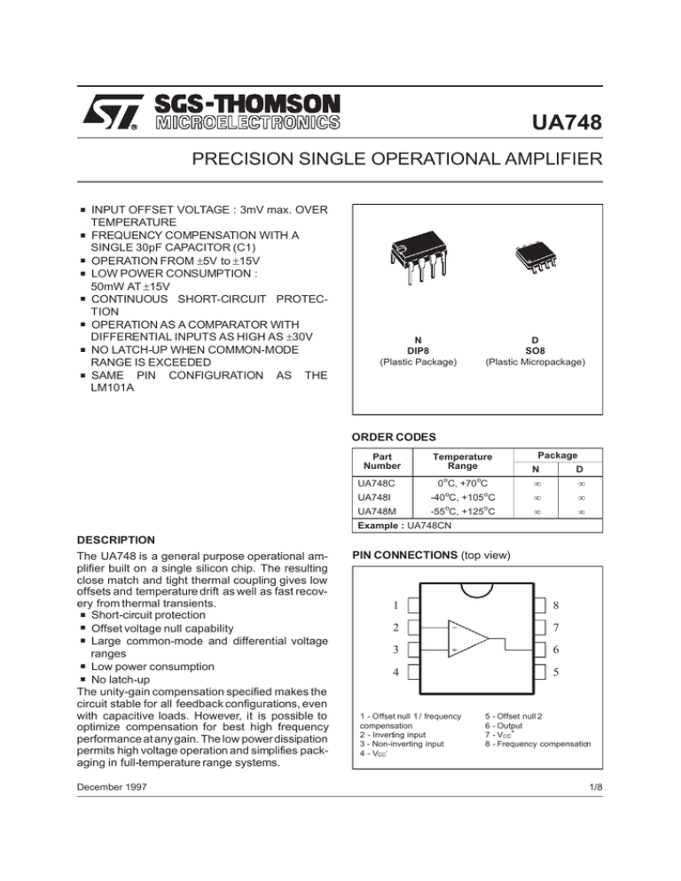
UA748
PRECISION SINGLE OPERATIONAL AMPLIFIER
.
.
..
.
.
.
.
INPUT OFFSET VOLTAGE : 3mV max. OVER
TEMPERATURE
FREQUENCY COMPENSATION WITH A
SINGLE 30pF CAPACITOR (C1)
OPERATION FROM ±5V to ±15V
LOW POWER CONSUMPTION :
50mW AT ±15V
CONTINUOUS SHORT-CIRCUIT PROTECTION
OPERATION AS A COMPARATOR WITH
DIFFERENTIAL INPUTS AS HIGH AS ±30V
NO LATCH-UP WHEN COMMON-MODE
RANGE IS EXCEEDED
SAME PIN CONFIGURATION AS THE
LM101A
N
DIP8
(Plastic Package)
D
SO8
(Plastic Micropackage)
ORDER CODES
Part
Number
Package
Temperature
Range
o
N
o
D
UA748C
0 C, +70 C
•
•
UA748I
-40oC, +105oC
•
•
UA748M
-55oC, +125oC
•
•
Example : UA748CN
DESCRIPTION
The UA748 is a general purpose operational amplifier built on a single silicon chip. The resulting
close match and tight thermal coupling gives low
offsets and temperature drift as well as fast recovery from thermal transients.
Short-circuit protection
Offset voltage null capability
Large common-mode and differential voltage
ranges
Low power consumption
No latch-up
The unity-gain compensation specified makes the
circuit stable for all feedback configurations, even
with capacitive loads. However, it is possible to
optimize compensation for best high frequency
performance at any gain. The low power dissipation
permits high voltage operation and simplifies packaging in full-temperature range systems.
..
.
..
December 1997
PIN CONNECTIONS (top view)
1
8
2
7
3
6
4
5
1 - Offset null 1 / frequency
compensation
2 - Inverting input
3 - Non-inverting input
4 - VCC-
5
6
7
8
- Offset null 2
- Output
- VCC+
- Frequency compensation
1/8
UA748
SCHEMATIC DIAGRAM
ABSOLUTE MAXIMUM RATINGS
Symbol
Parameter
UA748M
UA748C
Unit
Supply Voltage
±22
V
Vid
Differential Input Voltage
±30
V
Vi
Input Voltage
±15
V
Power Dissipation
500
mW
Ptot
Output Short-circuit Duration
2/8
UA748I
Vcc
Infinite
Toper
Operating Free Air Temperature Range
-55 to +125
-40 to +105
0 to +70
o
Tstg
Storage Temperature Range
-65 to +150
-65 to +150
-65 to +150
o
C
C
UA748
ELECTRICAL CHARACTERISTICS
±5V ≤ VCC ≤ ±20V, C1 = 30pF, Tamb = +25oC (unless otherwise specified)
Symbol
Vio
Iio
Iib
Avd
SVR
ICC
Parameter
Max.
Input Offset Voltage (RS ≤ 10kΩ)
o
Tamb = +25 C
Tmin. ≤ Tamb ≤ Tmax.
0.2
Input Offset Current
Tamb = +25oC
Tmin. ≤ Tamb ≤ Tmax.
Input Bias Current
Tamb = +25oC
Tmin. ≤ Tamb ≤ Tmax.
KOV
25
75
10
70
250
300
1.5
10
20
2
50
70
nA
nA
96
70
70
96
V/mV
dB
Supply Current, no load
Tamb = +25oC
Tmin. ≤ Tamb ≤ Tmax.
mA
1.8
3
3
±15
±15
1.8
V
dB
96
Output Short-circuit Current (V CC = ±15V)
10
30
Output Voltage Swing (VCC = ±15V)
o
RL = 10kΩ
Tamb = +25 C
R L = 2kΩ
RL = 10kΩ
Tmin. ≤ Tamb ≤ Tmax.
R L = 2kΩ
12
10
12
10
Slew Rate
(Vi = ±10V, R L =2kΩ, CL= 100pF, unity gain)
0.25
70
70
96
10
30
14
13
12
10
12
10
14
13
0.5
0.25
0.5
50
50
mA
V
V/µs
Rise Time
(Vi = ±20mV, RL = 2kΩ, CL = 100pF, unity gain)
0.3
0.3
Overshoot
(Vi = 20mV, R L = 2kΩ, CL = 100pF, unity gain)
5
5
Total Harmonic Distortion
(f = 1kHz, AV = 20dB, RL =2kΩ, VO = 2VPP,CL =
100pF)
3
3
±15
±15
80
80
Gain Bandwidth Product
(Vi = 10mV, RL = 2kΩ, CL= 100pF, f = 100kHz)
Unit
mV
80
80
Output Resistance (VCC = ±15V)
DIio
7.5
10
Supply Voltage Rejection Ratio (RS ≤ 10kΩ)
Tamb = +25oC
Tmin. ≤ Tamb ≤ Tmax.
Input Impedance (VCC = ±15V)
DV io
2
10
Ro
THD
2
3
25
15
ZI
GBP
Max.
100
Common-mode Rejection Ratio (R S ≤ 10kΩ)
o
Tamb = +25 C
Tmin. ≤ Tamb ≤ Tmax.
tr
Typ.
50
25
CMR
SR
Min.
Large Signal Voltage Gain *
(VCC = ±15V, VO ±10V, R L = 2kΩ)
o
Tamb = +25 C
Tmin. ≤ Tamb ≤ Tmax.
Input Common Mode Voltage Range (VCC =
±20V)
Tamb = +25oC
Tmin. ≤ Tamb ≤ Tmax.
±VOPP
Min.
UA748C
Typ.
Vicm
IOS
UA748I/M
µs
%
1.5
4
1.5
75
4
MΩ
Ω
75
MHz
0.5
1
0.5
1
%
0.015
0.015
o
Input Offset Current Drift
o
25 C ≤ Tamb ≤ Tmax.
Tmin. ≤ Tamb ≤ Tmax.
pA/ C
10
20
100
200
10
20
300
600
Input Offset Voltage Drift
Tmin. ≤ Tamb ≤ Tmax.
3
15
6
30
o
µV/ C
3/8
UA748
4/8
UA748
5/8
UA748
6/8
UA748
PACKAGE MECHANICAL DATA
8 PINS - PLASTIC DIP
Dim.
Millimeters
Min.
A
Typ.
Min.
3.32
a1
0.51
B
1.15
b
b1
Typ.
0.131
1.65
0.045
0.065
0.356
0.55
0.014
0.022
0.204
0.304
0.008
0.012
10.92
7.95
9.75
0.430
0.313
0.384
e
2.54
0.100
e3
7.62
0.300
e4
7.62
F
Z
0.300
6.6
i
L
Max.
0.020
D
E
Inches
Max.
0260
5.08
3.18
3.81
1.52
0.200
0.125
0.150
0.060
7/8
UA748
PACKAGE MECHANICAL DATA
8 PINS - PLASTIC MICROPACKAGE (SO)
Dim.
A
a1
a2
a3
b
b1
C
c1
D
E
e
e3
F
L
M
S
Min.
Millimeters
Typ.
0.1
0.65
0.35
0.19
0.25
Max.
1.75
0.25
1.65
0.85
0.48
0.25
0.5
Min.
Inches
Typ.
0.026
0.014
0.007
0.010
Max.
0.069
0.010
0.065
0.033
0.019
0.010
0.020
0.189
0.228
0.197
0.244
0.004
o
45 (typ.)
4.8
5.8
5.0
6.2
1.27
3.81
3.8
0.4
0.050
0.150
4.0
1.27
0.6
0.150
0.016
0.157
0.050
0.024
o
8 (max.)
Information furnished is believed to be accurate and reliable. However, SGS-THOMSON Microelectronics assumes no responsibility
for the consequences of use of such information nor for any infringement of patents or other rights of third parties which may result
from its use. No license is granted by implication or otherwise under any patent or patent rights of SGS-THOMSON Microelectronics.
Specifications mentioned in this publication are subject to change without notice. This publication supersedes and replaces all
information previously supplied. SGS-THOMSON Microelectronics products are not authorized for use as critical components in life
support devices or systems without express written approval of SGS-THOMSON Microelectronics.
1997 SGS-THOMSON Microelectronics – Printed in Italy – All Rights Reserved
SGS-THOMSON Microelectronics GROUP OF COMPANIES
Australia - Brazil - Canada - China - France - Germany - Italy - Japan - Korea - Malaysia - Malta - Morocco
The Netherlands - Singapore - Spain - Sweden - Switzerland - Taiwan - Thailand - United Kingdom - U.S.A.
8/8


