TQP4M3019
Data Sheet
SP3T High Power 2.6V 2x2 mm CDMA Antenna Switch
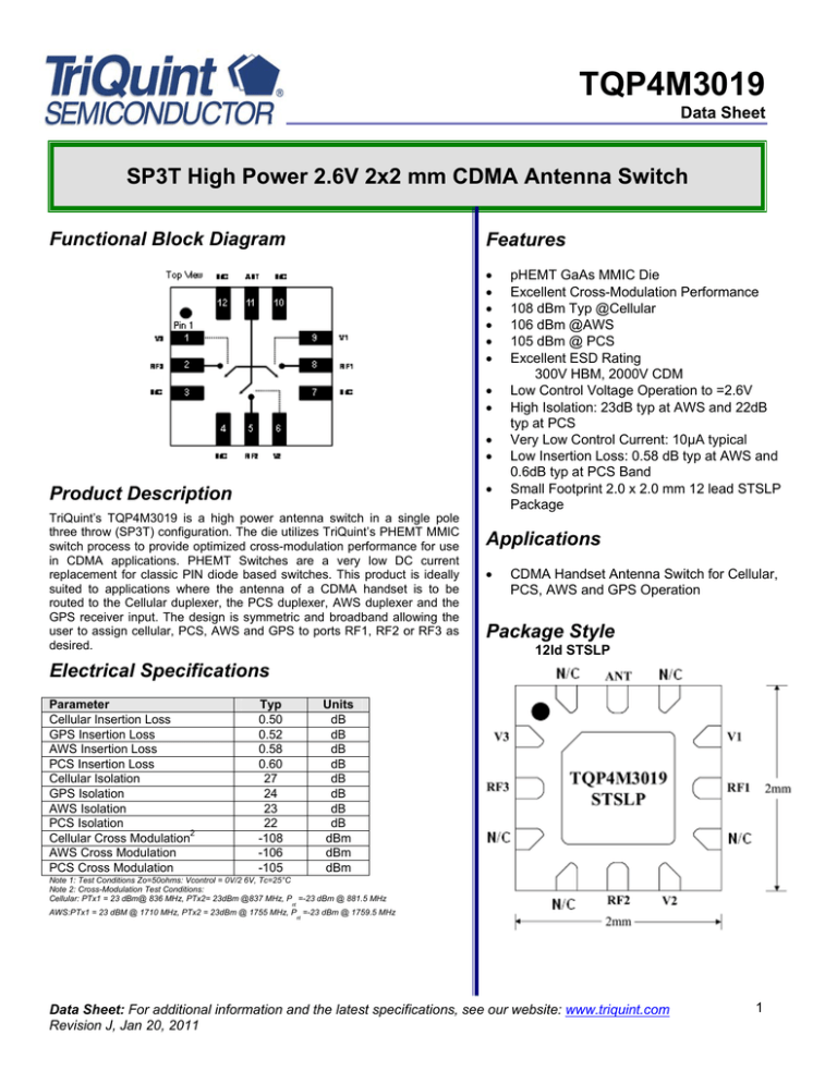
Functional Block Diagram
Features
Product Description
TriQuint’s TQP4M3019 is a high power antenna switch in a single pole
three throw (SP3T) configuration. The die utilizes TriQuint’s PHEMT MMIC
switch process to provide optimized cross-modulation performance for use
in CDMA applications. PHEMT Switches are a very low DC current
replacement for classic PIN diode based switches. This product is ideally
suited to applications where the antenna of a CDMA handset is to be
routed to the Cellular duplexer, the PCS duplexer, AWS duplexer and the
GPS receiver input. The design is symmetric and broadband allowing the
user to assign cellular, PCS, AWS and GPS to ports RF1, RF2 or RF3 as
desired.
pHEMT GaAs MMIC Die
Excellent Cross-Modulation Performance
108 dBm Typ @Cellular
106 dBm @AWS
105 dBm @ PCS
Excellent ESD Rating
300V HBM, 2000V CDM
Low Control Voltage Operation to =2.6V
High Isolation: 23dB typ at AWS and 22dB
typ at PCS
Very Low Control Current: 10µA typical
Low Insertion Loss: 0.58 dB typ at AWS and
0.6dB typ at PCS Band
Small Footprint 2.0 x 2.0 mm 12 lead STSLP
Package
Applications
CDMA Handset Antenna Switch for Cellular,
PCS, AWS and GPS Operation
Package Style
12ld STSLP
Electrical Specifications
Parameter
Cellular Insertion Loss
GPS Insertion Loss
AWS Insertion Loss
PCS Insertion Loss
Cellular Isolation
GPS Isolation
AWS Isolation
PCS Isolation
Cellular Cross Modulation2
AWS Cross Modulation
PCS Cross Modulation
Typ
0.50
0.52
0.58
0.60
27
24
23
22
-108
-106
-105
Units
dB
dB
dB
dB
dB
dB
dB
dB
dBm
dBm
dBm
Note 1: Test Conditions Zo=50ohms: Vcontrol = 0V/2 6V, Tc=25°C
Note 2: Cross-Modulation Test Conditions:
Cellular: PTx1 = 23 dBm@ 836 MHz, PTx2= 23dBm @837 MHz, P =-23 dBm @ 881.5 MHz
nt
AWS:PTx1 = 23 dBM @ 1710 MHz, PTx2 = 23dBm @ 1755 MHz, P =-23 dBm @ 1759.5 MHz
nt
Data Sheet: For additional information and the latest specifications, see our website: www.triquint.com
Revision J, Jan 20, 2011
1
TQP4M3019
Data Sheet
SP3T High Power 2.6V 2x2 mm CDMA Antenna Switch
Absolute Maximum Ratings
Symbol
Parameter
PIN MAX
Maximum Input Power
VCTRL
Control Voltage
TC
Case Temperature, Survival
TSTG
Storage Temperature
Note: The part may not survive all maximums applied simultaneously
Absolute Maximum Value
+38
+/-6
-40 to +85
-40 to +150
Units
dBm
VDC
°C
°C
Electrical Characteristics 1,2
Parameter (all paths)
Cellular Insertion Loss
GPS Insertion Loss
AWS Insertion Loss
PCS Insertion Loss
Cellular Isolation
GPS Isolation
AWS Isolation
PCS Isolation
Cellular CrossModulation
AWS Cross-Modulation
Test Conditions
Antenna to Selected RF Port (824 – 894 MHz)
Antenna to Selected RF Port (1574 – 1577 MHz)
Antenna to Selected RF Port (1710 – 1755 MHz)
Antenna to Selected RF Port (1850 – 1990 MHz)
RF Off Port to Selected RF Port (824 – 894 MHz)
RF Off Port to Selected RF Port (1574 – 1577 MHz)
RF Off Port to Selected RF Port (1710 – 1755 MHz)
RF Off Port to Selected RF Port (1850 – 1990 MHz)
PTx1=23 dBm,@836 MHz, PTx2=23dBm@837MHz, Pint=23 dBm@881.5 Mz
PTx1=23dBm,@1725.5 MHz, PTx2=23dBm@1727MHz,
Pint=-23 dBm@1759.5 Mz
PCS Cross-Modulation
PTx1=23 dBm,@1879.5 MHz, PTx2=23dBm@1880.5MHz,
Pint=-23 dBm@1960 Mz
Cellular IIP3
Tow tones; +23 dBm each; 837 MHz and 838 MHz
AWS IIP3
Tow tones; +23 dBm each; 1727 MHz and 1760 MHz
PCS IIP3
Tow tones; +23 dBm each; 1880 MHz and 1881 MHz
2nd Harmonic
Cellular; @ +25.5 dBm input
2nd Harmonic
AWS; @ +25 dBm input
2nd Harmonic
PCS; @ +24 dBm input
3rd Harmonic
Cellular; @ +25.5 dBm input
3rd Harmonic
AWS; @ +25 dBm input
3rd Harmonic
PCS; @ +24 dBm input
P-0.1 dB
Cellular
P-01 dB
AWS
P-01 dB
PCS
Return Loss
0.5 to 2.0 GHz
Leakage Current
Trise, Tfall
10% to 90% RF, 90% to 10% RF
Ton, Toff
50% control to 90% RF, and 50% control to 10% RF
Note 1: External DC Blocking capacitors are required at all RF ports.
Note 2: Test Conditions Zo = 50 ohms,; Vcontrol = 0V/2.6V, Tc=25 °C.
Units
dB
dB
dB
dB
dB
dB
dB
dB
dBm
Min
Typ
0.50
0.52
0.58
0.60
27
24
23
22
-108
-100
dBm
-106
-100
dBm
-105
-100
dBm
dBm
dBm
dBc
dBc
dBc
dBc
dBc
dBc
dBm
dBm
dBm
dB
µA
µS
µS
+66
+66
+66
-93
-93
-93
-93
-93
-95
+34
+34
+34.5
-25
10
25
20
20
20
Data Sheet: For additional information and the latest specifications, see our website: www.triquint.com
Revision J, Jan 20, 2011
Max
1
1
2
TQP4M3019
Data Sheet
SP3T High Power 2.6V 2x2 mm CDMA Antenna Switch
Application Example
AWS/PCS/CDMA with GPS
GPS Rx
LNA
PCS Tx/Rx
PCS
Duplexer
LNA
SP3T SWITCH
V1
V2
AWS
Duplexer
Cellular
Duplexer
CELLULAR Tx/Rx
Rx
PCS
PA
Tx
LNA
AWS Tx/Rx
GPS
Rx
AWS
PA
Tx
LNA
Rx
CELLULAR
PA
Tx
V3
Truth Table 1,2,3,4,5
V1
1
0
0
V2
0
1
0
V3
0
0
1
ANT RF1
On
Off
Off
ANT RF2
Off
On
Off
ANT RF3
Off
Off
On
PIN Descriptions1,2,3,4,5
PAD Number
1
2
3
4
5
6
7
8
9
10
11
12
PAD Name
V3
RF3
N/C
N/C
RF2
V2
N/C
RF1
V1
N/C
ANT
N/C
Description
Control RF Port 3
RF Port 3
No Connection
No Connection
RF Port 2
Control RF Port 2
No Connection
RF Port 1 Port
Control RF Port 1
No Connection
Antenna
No Connection
Note 1:State f = +26V,state 0=0V, Note2:Differential Voltage from State to State 0 must be a minimum of 26V; Note 3:DC grounding is not required.
Control voltages applied to pins 1,6 and 9 are differential being 0 volts and 26 volts nominally. Note 4: The package center paddle is n/c = no
connection and not grounded as the preferred user configuration. RF performance figures are quoted with n/c; Note 5:
All pins including the package center paddle are n/c = no connection and not grounded as the preferred user configuration. Grounding an n/c will not prevent the switch operation but
may give a small degradation in RF performance depending on board layout. There are no internal connections between these pads and the die.
Data Sheet: For additional information and the latest specifications, see our website: www.triquint.com
Revision J, Jan 20, 2011
3
TQP4M3019
Data Sheet
SP3T High Power 2.6V 2x2 mm CDMA Antenna Switch
Typical Example
Data Sheet: For additional information and the latest specifications, see our website: www.triquint.com
Revision J, Jan 20, 2011
4
TQP4M3019
Data Sheet
SP3T High Power 2.6V 2x2 mm CDMA Antenna Switch
Demonstration Board Circuit
Notes:
1.
2.
3.
4.
Package Paddle should not be grounded for the best performance. See Application Note for details.
RF and DC ground are through pins 1, 6, and 9
Control line bypass caps, C2, C5 and C7 should be at least 5pF and may be larger if needed, depending on the
switching time required in the application. See Application Note for details.
R1, R2 and R3 are optional pull down resistors to ensure the “Off” legs of the switch are held to a low enough
voltage in circuits using “open collector” style control lines. These lines must be held close to zero volts when the
corresponding switch leg is “off” for proper operation of the switch. A nominal control voltage of +2.6V is applied to
V1, V2 or V3 corresponding to the “On” leg of the switch, with the other two pins held at nominally 0V. Only one
switch leg maybe “On” at any time.
Data Sheet: For additional information and the latest specifications, see our website: www.triquint.com
Revision J, Jan 20, 2011
5
TQP4M3019
Data Sheet
SP3T High Power 2.6V 2x2 mm CDMA Antenna Switch
Application Board Component Locations:
Data Sheet: For additional information and the latest specifications, see our website: www.triquint.com
Revision J, Jan 20, 2011
6
TQP4M3019
Data Sheet
SP3T High Power 2.6V 2x2 mm CDMA Antenna Switch
Recommended PCB Footprint for 12ld STSLP 2x2x0.57mm Package
Procedure:
PCB Layout:
Leads are to extend away from the pads – these should be the same shape and size to ensure equal solder coverage.
Solder Mask:
The solder mask opening should be offset from the package edges by 250µm.
Solder Stencil:
Center pad opening is about 30% of PCB pad size.
Data Sheet: For additional information and the latest specifications, see our website: www.triquint.com
Revision J, Jan 20, 2011
7
TQP4M3019
Data Sheet
SP3T High Power 2.6V 2x2 mm CDMA Antenna Switch
Part Marking Information:
WHITE INK OR LASER MARK
Line 1: 019 – Product Code
Line 2: XXX – Last 3 Char of TriQuint assembly lot number
Data Sheet: For additional information and the latest specifications, see our website: www.triquint.com
Revision J, Jan 20, 2011
8
TQP4M3019
Data Sheet
SP3T High Power 2.6V 2x2 mm CDMA Antenna Switch
Tape and Reel Information:
Material will be delivered in packaged form on tape and reel.
PART
CAVITY
FEATURE
LENGTH
WIDTH
DEPTH
PITCH
DISTANCE
CAVITY TO PERFORATION
BETWEEN
LENGTH DIRECTION
CENTERLINE
CAVITY TO PERFORATION
WIDTH DIRECTION
COVER TAPE
WIDTH
CARRIER TAPE WIDTH
CAVITY
BOTTOM HOLE DIAMETER
PERFORATION DIAMETER
PITCH
POSITION
SYMBOL SIZE (in) SIZE (mm)
A0
0.091
2.30
B0
0.091
2.30
K0
0.030
0.75
P1
0.157
4.00
P2
0.079
2.00
F
0.138
3.50
C
W
D1
D0
P0
E1
0.213
0.315
0.059
0.059
0.157
0.069
5.40
8.00
1.50
1.50
4.00
1.75
Data Sheet: For additional information and the latest specifications, see our website: www.triquint.com
Revision J, Jan 20, 2011
9
TQP4M3019
Data Sheet
SP3T High Power 2.6V 2x2 mm CDMA Antenna Switch
STSLP-12
PART
FEATURE
FLANGE DIAMETER
THICKNESS
SPACE BETWEEN FLANGE
HUB
OUTER DIAMETER
ARBOR HOLE DIAMETER
KEY SLIT WIDTH
KEY SLIT DIAMETER
7” Reel
SYMBOL SIZE (in) SIZE (mm)
A
6.969
177.0
W2
0.559
14.2
W1
0.346
8.8
N
2.283
58.0
C
0.512
13.0
B
0.079
2.0
D
0.787
20.0
Each reel shall be marked as specified in TriQuint specification 12M05019A73, Section 7.
Data Sheet: For additional information and the latest specifications, see our website: www.triquint.com
Revision J, Jan 20, 2011
10
TQP4M3019
Data Sheet
SP3T High Power 2.6V 2x2 mm CDMA Antenna Switch
Packaging and Ordering Information:
Additional Information 1
This part is compliant with RoHS directive (Restrictions on the Use of Certain Hazardous Substances in Electrical and
Electronic Equipment).
The part is rated Moisture Sensitivity Level at 260°C per JEDEC standard IPC/JEDEC J-STD-020.
_____________________________
1. For the latest specifications, additional product information, worldwide sales and distribution locations and
information about TriQuint:
Web: www.triquint.com
Tel: (503) 615-9000
Email: info_wireless@tqs.com
Fax: (503) 615-8902
For Technical questions and additional information on specific applications:
Email: info_wireless@tqs.com
The information provided herein is believed to be reliable. TriQuint assumes no liability for inaccuracies or omissions.
TriQuint assumes no responsibility for the use of this information, and all such information shall be entirely at the user’s
own risk. Prices and specifications are subject to change without notice. No patent rights or licenses to any of the
circuits described herein are implied or granted to any third party.
TriQuint does not authorize or warrant any TriQuint product for use in life-support devices and/or systems.
Copyright © 2005 TriQuint Semiconductor, Inc. All rights reserved
Data Sheet: For additional information and the latest specifications, see our website: www.triquint.com
Revision J, Jan 20, 2011
11

![dB = 10 log10 (P2/P1) dB = 20 log10 (V2/V1). dBm = 10 log (P [mW])](http://s2.studylib.net/store/data/018029789_1-223540e33bb385779125528ba7e80596-300x300.png)
