PTVA042502EC
PTVA042502FC
Thermally-Enhanced High Power RF LDMOS FET
250 W, 50 V, 470 – 806 MHz
Description
The PTVA042502EC and PTVA042502FC LDMOS FETs are designed
for use in power amplifier applications in the 470 MHz to 806 MHz
frequency band. Features include high gain and thermally-enhanced
package with bolt-down or earless flanges. Manufactured with Infineon's
advanced LDMOS process, these devices provide excellent thermal performance and superior reliability.
PTVA042502FC
Package H-37248-4
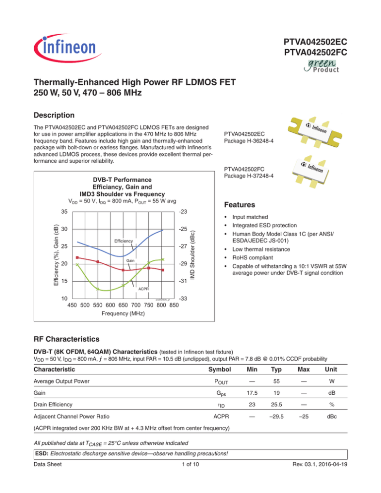
DVB-T Performance
Efficiancy, Gain and
IMD3 Shoulder vs Frequency
35
-23
30
-25
25
-27
Gain
20
-29
-31
15
Features
• Input matched
• Integrated ESD protection
IMD Shoulder (dBc)
Efficiency (%), Gain (dB)
VDD = 50 V, IDQ = 800 mA, POUT = 55 W avg
Efficiency
PTVA042502EC
Package H-36248-4
• Human Body Model Class 1C (per ANSI/
ESDA/JEDEC JS-001)
• Low thermal resistance
• RoHS compliant
• Capable of withstanding a 10:1 VSWR at 55W
average power under DVB-T signal condition
IMDACPR
Shoulder
10
ptva042502fc_g1
450 500 550 600 650 700 750 800 850
Frequency (MHz)
-33
RF Characteristics
DVB-T (8K OFDM, 64QAM) Characteristics (tested in Infineon test fixture)
VDD = 50 V, IDQ = 800 mA, ƒ = 806 MHz, input PAR = 10.5 dB (unclipped), output PAR = 7.8 dB @ 0.01% CCDF probability
Characteristic
Symbol
Min
Typ
Max
Unit
Average Output Power
POUT
—
55
—
W
Gain
Gps
17.5
19
—
dB
Drain Efficiency
hD
23
25.5
—
%
Adjacent Channel Power Ratio
ACPR
—
–29.5
–25
dBc
(ACPR integrated over 200 KHz BW at + 4.3 MHz offset from center frequency)
All published data at TCASE = 25°C unless otherwise indicated
ESD: Electrostatic discharge sensitive device—observe handling precautions!
Data Sheet
1 of 10
Rev. 03.1, 2016-04-19
PTVA042502EC
PTVA042502FC
DC Characteristics
Characteristic
Conditions
Symbol
Min
Typ
Max
Unit
Drain-Source Breakdown Voltage
VGS = 0 V, IDS = 10 mA
V(BR)DSS
105
—
—
V
Drain Leakage Current
VDS = 50 V, VGS = 0 V
IDSS
—
—
1.0
µA
VDS = 105 V, VGS = 0 V
IDSS
—
—
10.0
µA
On-State Resistance VGS = 10 V, VDS = 0.1 V
RDS(on)
—
0.1
—
W
Operating Gate Voltage
VDS = 50 V, IDQ = 800 mA
VGS
3.0
3.7
4.0
V
Gate Leakage Current
VGS = 10 V, VDS = 0 V
IGSS
—
—
1.0
µA
Maximum Ratings
Parameter
Symbol
Value
Unit
Drain-Source Voltage
VDSS
105
V
Gate-Source Voltage
VGS
–6 to +12
V
Junction Temperature
TJ
200
°C
Storage Temperature Range
TSTG
–65 to +150
°C
Thermal Resistance (TCASE = 70°C, 55 W CW) (S)
RqJC
0.4
°C/W
Ordering Information
Type and Version
Order Code
Package and Description
Shipping
PTVA042502EC V1 R0
PTVA042502ECV1R0XTMA1
H-36248-4, push-pull, bolt-down
Tape & Reel, 50pcs
PTVA042502EC V1 R250 PTVA042502ECV1R250XTMA1 H-36248-4, push-pull, bolt-down
Tape & Reel, 250pcs
PTVA042502FC V1 R0
H-37248-4, push-pull, earless
Tape & Reel, 50pcs
PTVA042502FC V1 R250 PTVA042502FCV1R250XTMA1 H-37248-4, push-pull, earless
Tape & Reel, 250pcs
Data Sheet
Rev. 03.1, 2016-04-19
PTVA042502FCV1R0XTMA1
2 of 10
PTVA042502EC
PTVA042502FC
Typical Performance (cont.)
Two Tone Drive-up
CW Performance
VDD = 50 V, IDQ = 800 mA, ƒ = 470 MHz,
1MHz Tone Spacing
26
50
40
24
Gain
22
30
20
20
Efficiency
16
29
33
37
41
45
-30
53
57
30
-40
-50
0
-60
30
35
40
-20
IM3 Low
-40
30
Efficiency
ptva042502fc_g4
45
50
55
Gain (dB)
45
Efficiency(%)
IMD Up & Low (dBc)
IM3 Up
40
0
10
Gain
5
15
0
IRL
10
15
5
0
0
-5
-10
250
350
450
550
650
750
ptva042502fc_g5
850
950
-15
Frequency (MHz)
Average Output Power (dBm)
Data Sheet
55
25
20
35
ptva042502fc_g3
VDD = 50 V, IDQ = 800 mA
60
30
50
Small Signal CW
Gain & Input Return Loss
VDD = 50 V, IDQ = 800 mA, ƒ = 806 MHz,
1MHz Tone Spacing
-50
45
Average Output Power (dBm)
Two Tone Drive-up
-30
15
Efficiency
Output Power (dBm)
-60
45
IM3 Low
10
ptva042502fc_g2
49
IM3 Up
Input Return Loss (dB)
18
60
-20
Efficiency(%)
60
IMD Up & Low (dBc)
28
Efficiency (%)
Gain (dB)
VDD = 50 V, IDQ = 800mA, ƒ = 470 MHz
3 of 10
Rev. 03.1, 2016-04-19
PTVA042502EC
PTVA042502FC
Load Pull Performance
Pulsed CW signal: 16 µs, 10% duty cycle, 50 V, 100 mA
P1dB
Max Output Power
Max PAE
Freq
[MHz]
Zs
[W]
Zl
[W]
Gain
[dB]
POUT
[dBm]
POUT
[W]
PAE
[%]
Zl
[W]
Gain
[dB]
POUT
[dBm]
POUT
[W]
PAE
[%]
500
0.9 – j1.4
2.9 + j0.8
22.4
54.05
254
71.2
2.5 + j4.5
24.6
50.59
115
79.5
600
0.7 – j2.0
2.2 + j0.8
21.1
52.15
164
61.8
2.2 + j3.6
23.4
49.27
85
76.3
700
1.4 – j2.8
2.1 + j0.8
20.5
52.64
184
59.6
1.9 + j3.4
22.9
49.97
99
75.3
859
3.7 – j4.9
2.0 + j0.2
19.1
52.38
173
62.2
1.8 + j1.9
21.2
50.44
111
74.1
POUT
[W]
PAE
[%]
Pulsed CW signal: 16 µs, 10% duty cycle, 50 V, 100 mA
P3dB
Max Output Power
Zs
[W]
Freq
[MHz]
Zl
[W]
Gain
[dB]
POUT
[dBm]
Max PAE
POUT
[W]
PAE
[%]
Zl
[W]
Gain
[dB]
POUT
[dBm]
500
0.9 – j1.4
2.9 + j0.6
20.3
54.58
287
74.1
2.6 + j4.1
22.4
51.49
141
80.0
600
0.7 – j2.0
2.3 + j0.7
19.0
52.77
189
62.2
2.3 + j3.2
21.1
50.39
109
76.9
700
1.4 – j2.8
2.2 + j0.7
18.4
53.34
216
60.2
1.8 + j3.2
20.7
50.60
115
75.8
859
3.7 – j4.5
2.0 + j0.1
17.0
53.11
205
63.9
1.8 + j1.8
19.1
51.08
128
73.6
All published data at TCASE = 25°C unless otherwise indicated
ESD: Electrostatic discharge sensitive device—observe handling precautions!
Data Sheet
4 of 10
Rev. 03.1, 2016-04-19
PTVA042502EC
PTVA042502FC
Reference Circuit , 470 – 806 MHz
RO4350, .020
(105)
RO4350, .020
(193)
VDD
C203 C204
C107
VGS
C201
C105
C108
C207
C103
R101
C117
RF_IN C119
C121
C208
C101
C114
C118
R103
C120
C115
C116
C112 C111
C211
C212 C213
C113
C104
R102
C215
C214
C217
C216
R201
C218
C220
C219
RF_OUT
C221
C102
C109
C209
VGS
C110
C106
C202
C205 C206
PTVA042502FC_IN_04
C210
VDD
PTVA042502FC_OUT_04
p t v a 0 4 2 5 0 2 f c _ C D _ 0 4 - 2 9 - 2 0 1 5
Reference circuit assembly diagram (not to scale)
Data Sheet
5 of 10
Rev. 03.1, 2016-04-19
PTVA042502EC
PTVA042502FC
Reference Circuit (cont.)
Reference Circuit Assembly
DUT
PTVA042502EC or PTVA042502FC
Test Fixture Part No.
LTN/PTVA042502EC V1 or LTN/PTVA042502FC V1
PCB
Rogers 4350, 0.508 mm [0.020”] thick, 2 oz. copper, εr = 3.66, ƒ = 470 – 806 MHz
Find Gerber files for this test fixture on the Infineon Web site at www.infineon.com/rfpower
Components Information
Component
Description
Manufacturer
P/N
C101, C102
Capacitor, 20 pF
ATC
ATC100A200JW150XB
C103, C104, C112, C115
Capacitor, 8.2 pF
ATC
ATC100A8R2JW150XB
C105, C106
Capacitor,120 pF
ATC
ATC700A120KP150XB
C107, C108, C109,
C110, C117, C121
Capacitor, 4.7 µF
Murata Electronics North America
GRM32ER71H475KA88L
C111, C113
Capacitor, 10 pF
ATC
ATC100A100JW150XB
C114, C116
Capacitor, 6.8 pF
ATC
ATC100A6R8JW150XB
C118, C120
Capacitor, 100 pF
ATC
ATC100A101JW150XB
C119
Capacitor, 91 pF
ATC
ATC100A910JW150XB
R101, R102
Resistor, 1K Ω
Panasonic Electronic Components
ERJ-8GEYJ102V
R103
Coax, 25 Ω
AMWAYE
UT-090C-25
C201, C202
Capacitor, 270 pF
ATC
ATC700A271KP150XB
C203, C204, C205,
C206, C220, C221
Capacitor, 4.7 µF
Murata Electronics North America
GRM32ER71H475KA88L
C207, C208, C209, C210
Capacitor, 100 µF
Panasonic Electronic Components
EEE-FP1V101AP
C211
Capacitor, 3.9 pF
ATC
ATC100A3R9CW150XB
C212
Capacitor, 6.8 pF
ATC
ATC100A6R8JW150XB
C213, C215
Capacitor, 8.2 pF
ATC
ATC100A8R2JW150XB
C214
Capacitor, 5.6 pF
ATC
ATC100A5R6CW150XB
C216
Capacitor, 3.3 pF
ATC
ATC100A3R3CW150XB
C217, C218
Capacitor, 100 pF
ATC
ATC100A101JW150XB
C219
Capacitor, 91 pF
ATC
ATC100A910JW150XB
R201
Coax, 25 Ω
AMWAYE
UT-090C-25
Input
Output
Data Sheet
6 of 10
Rev. 03.1, 2016-04-19
PTVA042502EC
PTVA042502FC
Pinout Diagram (top view)
S
D1
D2
G1
G2
Pin
D1
D2
G1
G2
S
Description
Drain device 1
Drain device 2
Gate device 1
Gate device 2
Source (Flange)
H-36248-4_pd_10-02-2013
S
D1
D2
H-37248-4_pd_10-10-2012
G2
G1
Lead connections for PTVA042502EC and PTVA042502FC
Data Sheet
7 of 10
Rev. 03.1, 2016-04-19
PTVA042502EC
PTVA042502FC
Package Outline Specifications
Package H-36248-4
(8.89
[.350])
2X 45° X 2.72
[45° X .107]
(5.08
[.200])
CL
D1
2X 4.83±0.51
[.190±0.020]
D2
S
FLANGE 9.78
[.385]
LID 9.40
19.43±0.51
[.370]
[.765±0.020]
CL
G1
2X 12.70
[.500]
1.02
[.040]
2X R1.63
[R.064]
G2
4X R1.52
[R.060]
4X 3.81
[.150]
27.94
[1.100]
19.81±0.20
[.780±0.008]
SPH 1.57
[.062]
3.76±0.25
[.148±0.010]
H-36248-4_po_02.1_10-22-2013
CL
34.04
[1.340]
Data Sheet
DiagramNotes—unlessotherwisespecified:
1. InterpretdimensionsandtolerancesperASMEY14.5M-1994.
2. Primarydimensionsaremm.Alternatedimensionsareinches.
3. Alltolerances±0.127[.005]unlessspecifiedotherwise.
4. Pins:D1,D2–drains;G1,G2–gates;S–source.
5. Leadthickness:0.10+0.076/–0.025mm[0.004+0.003/–0.001inch].
6. Goldplatingthickness:1.14±0.38micron[45±15microinch].
8 of 10
Rev. 03.1, 2016-04-19
PTVA042502EC
PTVA042502FC
Package Outline Specifications (cont.)
Package H-37248-4
(8.89
[.350])
(5.08
[.200])
2X 45° X 2.72
[45° X .107]
+0.13
-0.38
+0.005
[ R.030 -0.015 ]
4X R0.76
2X 4.83±0.51
[.190±0.020]
FLANGE 9.78
[.385]
CL
D1
D2
LID 9.40
[.370]
19.43±0.51
[.765±0.020]
CL
G1
G2
4X 3.81
[.150]
2X 12.70
[.500]
SPH 1.57
[.062]
19.81±0.20
[.780±0.008]
1.02
[.040]
0.0381 [.0015] -A-
H-37248-4_po_02_01-09-2013
3.76±0.25
[.148±0.010]
S
CL
20.57
[.810]
DiagramNotes—unlessotherwisespecified:
1. InterpretdimensionsandtolerancesperASMEY14.5M-1994.
2. Primarydimensionsaremm.Alternatedimensionsareinches.
3. Alltolerances±0.127[.005]unlessspecifiedotherwise.
4. Pins:D1,D2–drains;G1,G2–gates;S–source.
5. Leadthickness:0.10+0.076/–0.025mm[0.004+0.003/–0.001inch].
6. Goldplatingthickness:1.14±0.38micron[45±15microinch].
Find the latest and most complete information about products and packaging at the Infineon Internet page
http://www.infineon.com/rfpower
Data Sheet
9 of 10
Rev. 03.1, 2016-04-19
PTVA042502EC/FC V1
Revision History
Revision
Date
Data Sheet Type
Page
Subjects (major changes since last revision)
01
2012-09-19
Preliminary
All
Data Sheet reflects preliminary specification
02
2013-10-01
Preliminary
1
3
1, 2, 4, 5
6
Updated DVB-T characteristics, updated frequency range
Updated DVB-T performance graphs
Added H-36248-4 package information, pinout diagram and package outline
Updated package outline specification
02.1
2013-10-20
Preliminary
1, 2
Removed obsolete Pulsed Characteristics from Features, Removed Obsolete Pulsed CW table
03
2014-05-26
Production
All
1, 2
3, 4
Data Sheet reflects released product specification
Updated Features, DVB-T Charateristics table, thermal resistance
Updated all grahps, added loadpull information
03.1
2016-04-19
Production
1, 2
Added ESD rating, updated ordering information
We Listen to Your Comments
Any information within this document that you feel is wrong, unclear or missing at all?
Your feedback will help us to continuously improve the quality of this document.
Please send your proposal (including a reference to this document) to:
highpowerRF@infineon.com
To request other information, contact us at:
+1 877 465 3667 (1-877-GO-LDMOS) USA
or +1 408 776 0600 International
Edition 2016-04-19
Published by
Infineon Technologies AG
85579 Neubiberg, Germany
© 2012 Infineon Technologies AG
All Rights Reserved.
Legal Disclaimer
The information given in this document shall in no event be regarded as a guarantee of conditions or characteristics.
With respect to any examples or hints given herein, any typical values stated herein and/or any information regarding the
application of the device, Infineon Technologies hereby disclaims any and all warranties and liabilities of any kind,
including without limitation, warranties of non-infringement of intellectual property rights of any third party.
Information
For further information on technology, delivery terms and conditions and prices, please contact the nearest
Infineon Technologies Office (www.infineon.com/rfpower).
Warnings
Due to technical requirements, components may contain dangerous substances. For information on the types in question,
please contact the nearest Infineon Technologies Office.
Infineon Technologies components may be used in life-support devices or systems only with the express written approval of Infineon Technologies, if a failure of such components can reasonably be expected to cause the failure of that life-support device
or system or to affect the safety or effectiveness of that device or system. Life support devices or systems are intended to be
implanted in the human body or to support and/or maintain and sustain and/or protect human life. If they fail, it is
reasonable to assume that the health of the user or other persons may be endangered.
Data Sheet
10 of 10
Rev. 03.1, 2016-04-19


