ISSN: 2278 – 7798
International Journal of Science, Engineering and Technology Research (IJSETR)
Volume 5, Issue 8, August 2016
Pipelined 32bit RISC MIPS Processor on Spartan6
FPGA
Pranjali S. Kelgaonkar, Prof. Shilpa Kodgire
Abstract-- The main aim of the project is design and
implementation of the 32-bit RISC MIPS processor on Spartan6
FPGA. The project involves simulation and synthesis of a
processor. A Reduced Instruction Set compiler (RISC) is a
microprocessor that had been designed to perform a small set of
instructions, with the aim of increasing the overall speed of the
processor. The idea of this project was to create a RISC MIPS
processor as a building block in Verilog HDL. Each block is
separated by pipeline to speed up the processor. The project is
useful in the systems, where a problem is easy to solve in software
but hard to solve with control logic. However, high level of
complexity is easier to implement the function in software. The
processor implemented on Spartan 6 Digilent Board and designed
with Verilog HDL, synthesized using XILINX 14.2. The objective
of project is to increase the speed and reduce the power
consumption. Single cycle execution method applied to complete
one instruction through all stages.
Keywords– FPGA, MIPS, RISC, soc, spartan-6, xilinx14.2
I.
INTRODUCTION
Instruction format [4][13].Processor is using a large number of
instruction. Instruction set is expandable [5][14].Four stage
pipelines used. 8bit and 16 bit instruction set is used to access
logical, arithmetic and memory, jump instructions [6]. Spartan
2 is considered to design. Simulation and synthesis done on
XILINX ISE [6]. For sign multiplication, booth multiplier is
used [7]. The paper has more coverage to the instruction set
[8]. 20 bit instruction format considered [9] .For temporary
data storage internal register bank is used, to avoid access of
memory again and again [11][13].Processor is designed on
account the consideration of automation [10].
III. SYSTEM MODELING
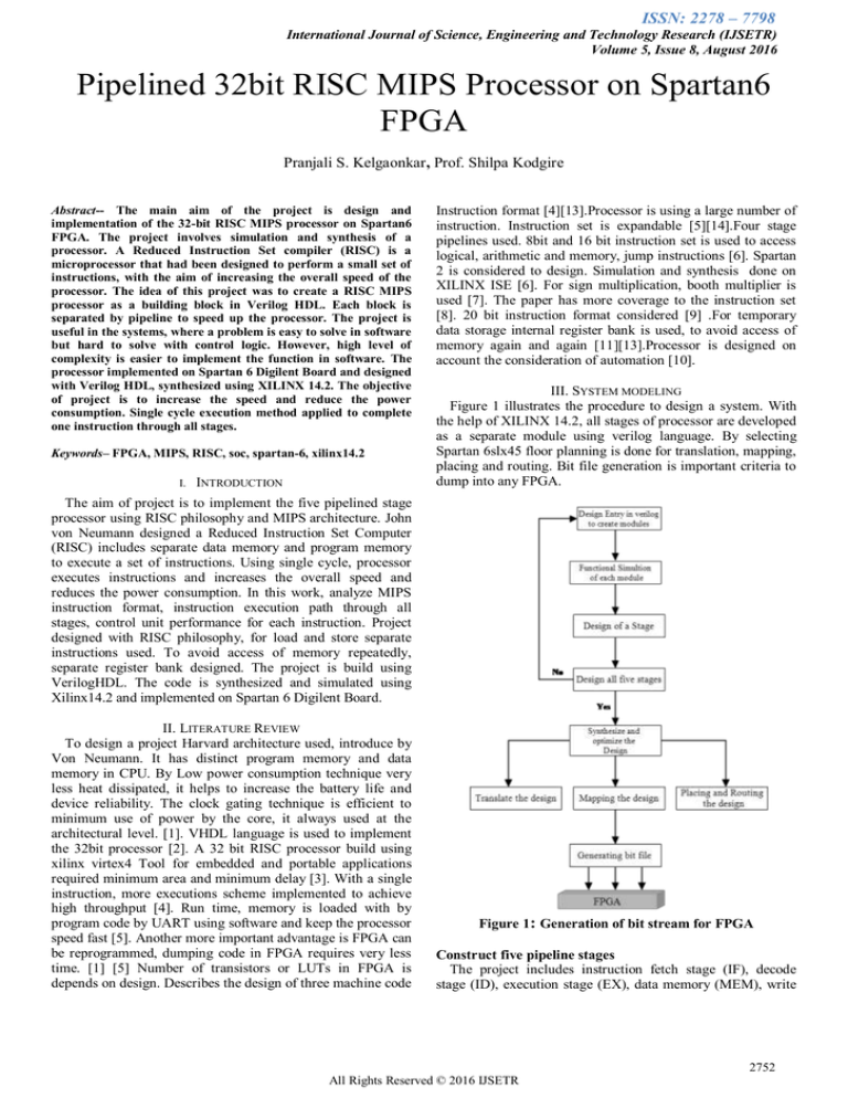
Figure 1 illustrates the procedure to design a system. With
the help of XILINX 14.2, all stages of processor are developed
as a separate module using verilog language. By selecting
Spartan 6slx45 floor planning is done for translation, mapping,
placing and routing. Bit file generation is important criteria to
dump into any FPGA.
The aim of project is to implement the five pipelined stage
processor using RISC philosophy and MIPS architecture. John
von Neumann designed a Reduced Instruction Set Computer
(RISC) includes separate data memory and program memory
to execute a set of instructions. Using single cycle, processor
executes instructions and increases the overall speed and
reduces the power consumption. In this work, analyze MIPS
instruction format, instruction execution path through all
stages, control unit performance for each instruction. Project
designed with RISC philosophy, for load and store separate
instructions used. To avoid access of memory repeatedly,
separate register bank designed. The project is build using
VerilogHDL. The code is synthesized and simulated using
Xilinx14.2 and implemented on Spartan 6 Digilent Board.
II. LITERATURE REVIEW
To design a project Harvard architecture used, introduce by
Von Neumann. It has distinct program memory and data
memory in CPU. By Low power consumption technique very
less heat dissipated, it helps to increase the battery life and
device reliability. The clock gating technique is efficient to
minimum use of power by the core, it always used at the
architectural level. [1]. VHDL language is used to implement
the 32bit processor [2]. A 32 bit RISC processor build using
xilinx virtex4 Tool for embedded and portable applications
required minimum area and minimum delay [3]. With a single
instruction, more executions scheme implemented to achieve
high throughput [4]. Run time, memory is loaded with by
program code by UART using software and keep the processor
speed fast [5]. Another more important advantage is FPGA can
be reprogrammed, dumping code in FPGA requires very less
time. [1] [5] Number of transistors or LUTs in FPGA is
depends on design. Describes the design of three machine code
Figure 1: Generation of bit stream for FPGA
Construct five pipeline stages
The project includes instruction fetch stage (IF), decode
stage (ID), execution stage (EX), data memory (MEM), write
2752
All Rights Reserved © 2016 IJSETR
ISSN: 2278 – 7798
International Journal of Science, Engineering and Technology Research (IJSETR)
Volume 5, Issue 8, August 2016
back (WB) stages. For jump instruction separate block is
designed. Pipeline consists of the overlapping of set of
instructions. Pipeline reduces the execution time of
instructions.
Figure 3: Instruction Types
Figure 2: Five Stage Pipeline
The processor executes an instruction in single cycle. Each
instruction passes through all stages or passes according to
instruction. Program counter loaded with the address it acts as
a pointer to the program memory.
Instruction Fetch
The program memory loaded with Instructions. The
instruction fetched from memory. Each time program counter
has the address of memory location. All fetched instructions
passed to decoder stage through latch.
Instruction Decode
The Instruction Decode stage decodes the instruction. The
six bit Opcode is passed to the control unit to generate the
signals according to instruction code. The data passed through
decoder latch for execution as per signals generated by control
unit. Sign extension unit used to extend the value according to
control signals. If instruction is load or store type, immediate
[15-0] bits extend to 32 bit for ALU. In decode stage Register
Bank performs as cache memory to store the data for fast
calculation.
Execute Stage
In Execute stage, the instructions are executed. All arithmetic
and logical operations perform by ALU. Type of operations
are addition, subtraction, AND, OR etc.
R-type performs the arithmetic and logical instruction
source and destination are declared in the instruction. Function
field [6-0] decides the action to taken by ALU. The instruction
register address fields Rs [25-21], Rt [20-16] and Rd [15-11]
are used to address the register file. The two independent
register reads and one register write in one clock cycle.
I-Type performs the Load and Store Operations. Memory
address is calculated by ALU. Result of ALU acts as pointer to
data memory. Read or write operation for memory is decided
by the control signals.
J-type performs jump instructions. It has only opcode and
26 immediate bits, contents the address of program memory
location to jump. Only IF stage and jump block is active,
remaining stages are inactive. For NOP, time progresses but no
action is taken by the processor, it consumes clock cycle, plays
important role in delay. For HALT, processor has to stop all
operations. For OUT, the action performed only by data
memory and saved data is on the out bus for peripherals.
IV. PERFORMANCE ANALYSIS
Software Hardware Implementation
For this Project, Verilog is used to design modules, several
modules are integrated in single module. To simulate the
circuit, it needs to write a test bench for getting different
output for different inputs at different interval. Xilinx ISE
14.2,ISIM 14.2, to synthesize and simulate the design.
Translation, mapping and routing done using Xilinx ISE 14.2
and PlanAhead 14.2. Finally bit file is created to program
Spatran-6 xc6slx45 Fpga.
The ADEPT recommended by Diligent Spartan-6 platform,
is freely available on Digilent website, used to dump .bit file
in the chip.
Memory Access
Data memory is storage device accessed as per the load and
store instruction. For load instruction, Data is loaded to
register bank from memory. For store instruction, current data
stores in the data memory.
Write back stage
The result writes back to the register file. All instructions
passed via Write back stage. Except nops and store type of
instruction.
Instruction Types
Three Instruction types are used for designing and
programming purpose. 32bits are divided in groups and named
according to instruction. Opcode group has [31-26] bits, sent
to a control unit to send the control signals as type of
instruction to execute.
Figure 4: Multiplication of two bit output on Digilent
Spartan-6 Board.
2753
All Rights Reserved © 2016 IJSETR
ISSN: 2278 – 7798
International Journal of Science, Engineering and Technology Research (IJSETR)
Volume 5, Issue 8, August 2016
Output of 32-bit MIPS RISC Processor
The verilog code of each stage is pipelined then synthesized
and simulated on xilinx14.2 and ISIM simulator. Each stage
executed in synchronization with clock.
Figure 5: Output of 32-bit processor.
V. FUTURE DEVELPMENT
A Field-programmable Gate Array (FPGA) is an integrated
circuit designed to be configured by the customer or designer
after manufacturing hence field-programmable. The FPGA
configuration is generally specified using a hardware
description language (HDL), similar to that used for an
application-specific integrated circuit (ASIC). FPGAs can be
used to implement any logical function that an ASIC could
perform. Now my focus is, increasing the number of
instructions and implementation of input the user data from
user side..
[12] Digital Design – Morris Mano 5E.
[13] Mohit N. Topiwala, N. Saraswathi,Professor S.G, “Implementation of a
32-bit MIPS Based RISC Processor using Cadence”, 2014 IEEE
International Conference on Advanced Communication Control and
Computing Technologies (ICACCCT).
[14] S. P. Ritpurkar , Prof. M. N. Thakare, Prof. G. D. Korde “Design and
Simulation of 32-Bit RISC Architecture Based on MIPS using VHDL”,
2015 International Conference on Advanced Computing and
Communication Systems (ICACCS -2015), Jan. 05 – 07, 2015,
Coimbatore, INDIA.
[15] Mrs. Rupali S. Balpande, Mrs.Rashmi S. Keote, Design of FPGA based
Instruction Fetch & Decode Module of 32-bit RISC (MIPS)
Processor,2011 International Conference on Communication Systems
and Network Technologies, 978-0-7695-4437-3/11, 2011 IEEE.
Pranjali S. Kelgaonkar, pursuing ME(Embedded Systems), Department of
Electronics and Telecommunication Engineering, MIT, Aurangabad,
Maharashtra, India. research area :VLSI.
Prof. Shilpa Kodgire, Associate Prof.,Department of Electronics and
Telecommunication Engineering, MIT, Aurangabad, Maharashtra, India
research area :VLSI.
CONCLUSION
32 bit RISC Processor has been designed, using Xilinx 14.2.
The design has been achieved using Verilog HDL and
simulated with ISIM. Pipelined design of each module is
simulated successfully. Most of the goal is achieved and
simulation shows that the processor is working perfectly. Also
Spartan-6 is working as per the program code.
REFERENCES
Preetam Bhosale, Hari Krishna Murti, FPGA Implementation of Low
Power Pipelined 32-bit RISC Processor, IJITEE Volume-1,Issue-3,
August 2012.
[2] N.Alekya ,P.Ganesh Kumar,Design of 32-Bit Risc CPU Based on MIPS,
JGRCS Volume 2,No 9,September 2011
[3] Galani Tina G.,Riya Saini and R.D.Daruwala,Design and
Implementation of 32 – bit RISC Processor using Xilinx, IJITEE
Volume-5,Issue-1, August 2013
[4] J.Poornima, G.V.Ganesh, M.jyothi,M.Sahithi,A.jhansi RaniB. Raghu
Kanth, Design and Implementation of Pipelined 32-bit
Advanced
RISC Processor for Various D.S.P Applications", (IJCSIT) International
Journal of Computer Science and Information Technologies, Vol. 3 (1) ,
2012,3208-3213.
[5] Marri Mounika,Aleti Shankar, Design and implementation of 32-bit Risc
(MIOS) Processor, International Journal of Engineering Trends and
Technology (IJETT)-volume 4 Issue 10 –Oct2013.
[6] Navneet kaur, Adesh Kumar, Lipika Gupta,VHDL Design and Synthesis
of 64 bit RISC Processor System on Chip (SoC), IOSR Journal of VLSI
and Signal Processing (IOSR-JVSP) Volume 3, Issue 5 (Nov. – Dec.
2013), PP 31-42 e-ISSN: 2319 – 4200, p-ISSN No. : 2319 – 4197.
[7] R.Uma,Design and Performance Analysis of 8-bit RISC Processor using
Xilinx Tool, International Journal of Engineering Research and
Applications (IJERA) ISSN: 2248-9622 www.ijera.com Vol. 2, Issue 2,
Mar-Apr 2012, pp.053-058.
[8] Sagar Bhavsar, Akhil Rao, Abhishek Sen, Rohan Joshi, A 16-bit MIPS
Based Instruction Set Architecture for RISC Processor, International
Journal of Scientific and Research Publications, Volume 3, Issue 4, April
2013.
[9] Prof. Bruce Jacob, The RiSC-16 Instruction-Set Architecture, ENEE
446: Digital Computer Design, Fall 2000.
[10] Anand Nandakumar Shardul, 16-Bit RISC Processor Design for
Convolution Application, International Journal of Advancements in
Research & Technology, Volume 2, Issue 9, September-2013.
[11] Computer Organization and design – David A. Patterson,John
L.Hennessy.
[1]
2754
All Rights Reserved © 2016 IJSETR


