Two-Quadrant Analog Multiplier Project
advertisement
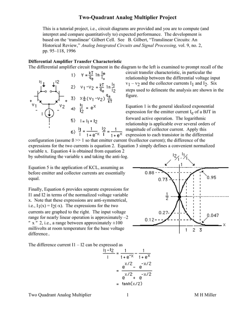
Two-Quadrant Analog Multiplier Project This is a tutorial project, i.e., circuit diagrams are provided and you are to compute (and interpret and compare quantitatively to) expected performance. The development is based on the ‘translinear’ Gilbert Cell. See B. Gilbert, “Translinear Circuits: An Historical Review,” Analog Integrated Circuits and Signal Processing, vol. 9, no. 2, pp. 95–118, 1996 Differential Amplifier Transfer Characteristic The differential amplifier circuit fragment in the diagram to the left is examined to prompt recall of the circuit transfer characteristic, in particular the relationship between the differential voltage input v1 – v2 and the collector currents I1 and I2. Six steps used to delineate the analysis are shown in the figure. Equation 1 is the general idealized exponential expression for the emitter current Ie of a BJT in forward active operation. The logarithmic relationship is applicable over several orders of magnitude of collector current. Apply this expression to each transistor in the differential configuration (assume ß >> 1 so that emitter current ≈ collector current); the difference of the expressions for the two currents is equation 2. Equation 3 simply defines a convenient normalized variable x. Equation 4 is obtained from equation 2 by substituting the variable x and taking the anti-log. Equation 5 is the application of KCL, assuming as before emitter and collector currents are essentially equal. Finally, Equation 6 provides separate expressions for I1 and I2 in terms of the normalized voltage variable x. Note that these expressions are anti-symmetrical, i.e., I1(x) = I2(-x). The expressions for the two currents are graphed to the right. The input voltage range for nearly linear operation is approximately –2 ≤ x ≤ 2, i.e., a range between approximately ±100 millivolts at room temperature for the base voltage difference.. The difference current I1 – I2 can be expressed as Two Quadrant Analog Multiplier 1 M H Miller Note that this expression, although it depends on the assumption ß >>1 does not depend on an incremental parameter assumption. For small arguments the value of the hyperbolic tangent is approximated by its argument, i.e., For x/2 <<1 I1 – I2 ≈ (qe/2kT)(v1 – v2) I Operated under the conditions as described the circuit is described as a ‘two-quadrant’ multiplier, i.e., operation is restricted to differential input voltages of a few millivolts or less and requires I > 0 (see shaded area in figure). Note that the amplifier differential mode maximum collector transconductance gain occurs at x=0 and is (for I2) with a similar expression for I1. This works out to about 10I amperes/volt at room temperature. The voltage gain depends on the size of the collector resistor through which the current flows. Note specifically that the gain depends on the DC bias current, and this current can be used, for example, as a gain control. Several illustrative applications follow. Analog Switch (Chopper) An illustrative differential amplifier circuit diagram is drawn to the right. (A unity gain voltage-controlled voltage source part E4 is used as an output device in place of a formal differential voltage follower to limit the parts count.) Note: Imagine S1 is the signal applied to the base input of Q3, and S2 is that applied to the base input of Q4. Note the following mathematical identities: S1 = (S1 + S2)/2 + (S1 - S2)/2 S2 = (S1 + S2)/2 – (S1 - S2)/2 The term (S1 + S2)/2 corresponds to a common mode input, and the differential amplifier circuit symmetry discriminates against amplification of this input term. The effective input component is the differential mode term (S1 - S2)/2. For the circuit as shown S1 = V1 and S2 = 0. Hence the single-ended input corresponds effectively to a differential mode input of ±V1/2. Amplifier gain is proportional to the bias current provided by Q5, and this is controlled through the V9 pulse voltage source. Two control voltages are to be used (separately) for illustration. First a pulse input is applied which simply switches the Q5 bias current from ≈ 3.44ma to zero (verify this). The voltage gain then is ≈ 68.9 (verify this), and for a 20 millivolts volt input the differential output voltage Two Quadrant Analog Multiplier 2 M H Miller would be ≈ 1.38v. Use as a bias current ‘modulating’ voltage a pulse waveform with a nominal period of 5 milliseconds, and a nominal duty factor of 60%. Use a sinusoidal signal frequency (V1) of 20 millivolts at 1 kHz. Compute performance (and interpret and compare quantitatively to expected performance) data similar to that shown below.) Analog Gain Control In the previous illustration the amplifier gain is switched between two extremes. The gain also may be varied continuously, as this next illustration shows. The circuit is the same as before, except that the modulating pulse source is replaced by a source providing a triangular voltage varying the gain approximately linearly between its peak value and cutoff. (The triangular waveform may be synthesized as a pulse with a twelve msecond pulse width, rise and fall times of 5.95msec respectively, and a pulse width of 100 µseconds. The PSpice computation for the output is drawn below. Compute (interpret and compare quantitatively to expected performance) data similar to that shown above.) Two Quadrant Analog Multiplier 3 M H Miller Amplitude Modulation (two quadrant) The trigonometric equivalence 2 sin(ωmt) sin(ωct) = cos((ωm+ωc) – cos((ωm-ωc)t is the mathematical basis of ‘amplitude modulation’, i.e., frequency shifting of two sinusoidal signals to form sum and difference frequencies. The higher frequency product signal (ωm+ωc) can be propagated as a radio wave more efficiently than the modulating signal (ωm) itself; the modulation can be recovered by a rectification and filtering process similar to that used in rectifiers. In practice the carrier would have a significantly higher frequency than the modulation; the choices made for this illustrative project however are adequate to show the basic modulation effect, and still provide a relative computational simplicity.) The carrier frequency used is 50kHz and the modulating frequency is 500Hz. The circuit is modified from that used before in two ways. First, as noted, the carrier signal is here a 50Khz, 100 millivolts sinusoid, and the modulating source is a 500 Hz sinusoidal source with amplitude 5v. In addition a simple half-wave rectifier and low-pass filter is added (upper right) to accept the differential output signal, to demodulate the modulated waveform, and to recover the modulation signal. The difference voltage between the Q3-Q4 collectors is plotted below. The high frequency carrier plot is a blur because of the scale involved. A plot on an expanded scale follows to indicate some of the finer structure of the waveform. Two Quadrant Analog Multiplier 4 M H Miller (Note: the filtering process may be viewed as first rectifying the signal to produce a unidirectional waveform, and then using an RC voltage divider with a time constant large enough (0.47 milliseconds) not to be able to follow the 50 KHz changes, but not so large as not to track the 500Hz variations. This separation is more effective the greater the difference in the frequencies involved.) Finally the rectified and filtered output waveform is plotted. Note: the DC component of the rectified waveform is ‘filtered out’ mathematically by having PSpice subtract the average. For comparison a scaled plot of the modulating waveform also is plotted. Compute (interpret and compare quantitatively to expected performance) data similar to those shown above.) Two Quadrant Analog Multiplier 5 M H Miller Four-Quadrant Analog Multiplier Amplitude Modulation (four quadrant) The preceding conclusions assume the differential input signal is small, i.e., less than about 0.5 millivolts at room temperature. And, in addition, the bias current necessarily is positive. It is from these constraints that the description ‘two quadrant’ is derived. So-called ‘fourquadrant’ multiplication is obtained by combining two two-quadrant multipliers as illustrated to the right. Q1– Q2 and Q3-Q4 respectively form a pair of crossconnected differential amplifiers, with the base signal v1 connected so that corresponding collector currents add. A third differential amplifier Q5-Q6 controls the bias current for the cross-connected differential amplifiers An analysis similar to that illustrated before is shown below. The analysis demonstrates that the difference current ia – ib is, assuming small-signal input conditions, proportional to the product of the differential input signals v1 and v2. A circuit diagram for an illustrative four-quadrant multiplier is drawn below. The input signals both are specified as 1kHz sinusoids, with amplitude of 50 millivolts, so that the output would be proportional to sin2 θ = (1 – cos 2θ)/2. The PSpice plot compares the differential output with a 1 kHz sinusoid to verify the frequency doubling. Two Quadrant Analog Multiplier 6 M H Miller First the difference current in the ‘bias current’ amplifier is plotted as a function of the (single-ended) bias voltage v(mod). The associated emitter current is nominally (12 –0.7)/1.5 = 7.5 ma, and the expected plot theoretically is a line with slope 7.5/(2)(26) = 0.014 ma/mv. For the data plotted next the two sinusoidal sources both were set to 29 millivolts, 1 kHz. The estimated output voltage amplitude is Two Quadrant Analog Multiplier 7 M H Miller For the next calculation, a doubly balanced modulator, the (car) frequency is set to 50 kHz, and the (mod) frequency to 500Hz. The anticipated output signal is 1.1 sin (2π.50kt) sin(2π.500t). Note that this form of a modulator produces an output absent a spectral term at the carrier frequency. Fine structure is shown in the next plot using an expanded time scale. Two Quadrant Analog Multiplier 8 M H Miller
