Structural changes of polycrystalline silicon layers during high
advertisement

Structural changes of polycrystalline silicon layers during high temperature
annealing
D. Lysáček, L. Válek
ON SEMICONDUCTOR CZECH REPUBLIC, Rožnov p. R.,
david.lysacek@onsemi.com
Abstract
The structure of undoped polycrystalline silicon films deposited by low pressure,
chemical vapor deposition has been investigated by x-ray diffraction and scanning
electron microscopy after high temperature annealing. The polycrystalline silicon films
deposited at 640°C are stable upon annealing to temperatures up to approximately 900°C.
Primary recrystallization has been observed between 900°C and 1150°C.
Introduction
After the polycrystalline silicon film has been deposited, it usually undergoes high
temperature processing during subsequent steps of the device fabrication. Changes in the
grain structure during these thermal cycles can significantly affect the properties of the
polycrystalline silicon layers and thereby performance of integrated circuits [1].
Changes in the structure of the polycrystalline silicon depend on the annealing conditions,
initial structure formed during the deposition and dopant present in the polycrystalline
silicon during annealing. The initial structure is determined by the deposition conditions,
primarily by the deposition temperature [2]. The presence of the n-type dopant enhances
the recrystallization process by enhancing the diffusion of the silicon self interstitials
across the grain boundaries [3, 4]. The boron doping has negligible effect on the
recrystallization process [1].
Experimental
The samples were produced in ON Semiconductor Czech Republic [5]. Silicon wafers
were sliced from a Czochralski-grown ingot heavily doped with antimony; resistivity of
the wafers was 10 – 20 mΩcm and crystallographic orientation was (100).
The polycrystalline silicon layers were grown by the Low Pressure Chemical Vapor
Deposition (LPCVD) technique using SiH4 as a source gas. The deposition temperature
was 640°C and the pressure 150 mTorr. The thickness of the layers was 1.1 µm.
The wafers were annealed in ambient atmosphere at 650°C, 900°C, 1050°C and 1150°C
for 0.5 hr, 2 hrs and 24 hrs, respectively.
The crystallographic orientation of the grains in the polycrystalline silicon films was
measured at the Masaryk University Brno, Czech Republic, by the x-ray diffraction with
CuKα radiation. The samples were tilted by 5° to reduce the substrate reflections. The
cross sections of the polycrystalline silicon layers were delineated by selective etching
and imaged on a JEOL JSM 5500 Scanning Electron Microscope with electron beam
acceleration voltage of 10 kV in ON Semiconductor Czech Republic [5].
Results and discussion
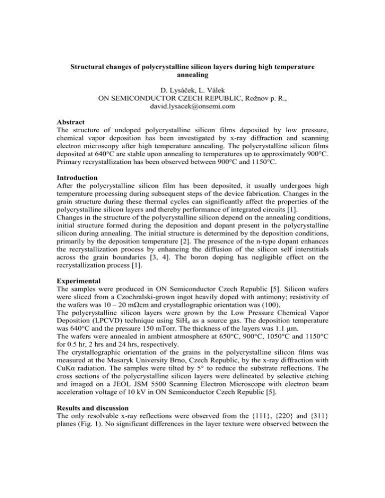
The only resolvable x-ray reflections were observed from the {111}, {220} and {311}
planes (Fig. 1). No significant differences in the layer texture were observed between the
polycrystalline silicon layers deposited on the bare silicon wafer and on the wafer
overcoated by the 100 nm thick silicon dioxide layer. This can be explained by the
presence of the native oxide on the surface of the bare wafer. In fact, polycrystalline
layers are always deposited on the silicon dioxide, unless they are grown in-situ after the
wafer etching. For the same reason, texture of the polycrystalline silicon layers is not
affected by the crystallographic orientation of the substrate.
30
30
(111)
650°C
(220)
(311)
20
15
10
5
900°C
25
Relative intensity
Relative intensity
25
20
(111)
(220)
15
(311)
10
5
0
0
Reference
0.5
2
24
Reference
Annealing time [hrs]
30
2
24
Annealing time [hrs]
30
1050°C
1150°C
25
20
(111)
(220)
15
(311)
10
Relative intensity
25
Relative intensity
0.5
20
(111)
(220)
15
(311)
10
5
5
0
0
Reference
0.5
2
Annealing time [hrs]
24
Reference
0.5
2
24
Annealing time [hrs]
Fig. 1 X-ray texture of the polycrystalline silicon layers after annealing at 650°C,
900°C, 1050°C and 1150°C for 0.5 hr, 2 hrs and 24 hrs, respectively.
The polycrystalline silicon films show only little structural changes for annealing
temperature up to 900°C. At 1050°C and above, significant changes appears. The <111>
texture increases significantly, <220> texture decrease slightly and <311> texture doesn’t
change. Thus significant changes in the grain structure do not occur until the annealing
temperature is increased above a critical value. In our case the critical temperature lies
between 900°C and 1050°C, which is in agreement with Kamins [6] who reported the
critical temperature of 1000°C. It is obvious that the grain structure depends mainly on
the annealing temperature, while annealing time in the range from 0.5 to 24 hrs has minor
influence.
Three different phenomena can influence the grain growth [1]. (a) The strain-induced
growth, where the grain size increases linearly with annealing time. (b) The grain
boundary-induced growth, where the driving force of recrystallization is inversely
proportional to the radius of curvature of the grain boundary, and the grain size increases
as the square root of the annealing time and (c) impurity drag, where impurities
incorporated at the grain boundary can retard the grain growth, which then exhibits a
cube-root time dependence of the grain size. Wada and Nishimatsu [3] reported the
driving force for the primary recrystallization to be the interface energy and the
elementary process behind the primary recrystallization is diffusion of silicon self
interstitials across the grain boundary region.
The dependence of the grain size on the annealing time and on the annealing temperature
(Fig. 2) shows that the grain size does not change significantly at the annealing
temperature up to 900°C even for the annealing time 24 hrs. Significant increase in the
grain size was observed after annealing at 1050°C and 1150°C.
Since the temperatures around 1100°C are commonly used in the process of integrated
circuit fabrication, grain size of the polycrystalline silicon layer can grow by the factor of
2-3 compared to its deposited size. This fact can significantly affect the properties of the
polycrystalline silicon layers and consequently performance of the integrated circuits.
0.7
0.6
Grain size [um]
Grain size [um]
0.6
0.7
a)
0.5
0.4
0.3
0.2
0.1
0
650
b)
0.5
0.4
0.3
0.5
0.2
2
900
0.1
24
1050
0
1150
Reference
0.5
2
Annealing time [hrs]
24
Reference
650
900
1050
1150
Annealing temperature [°C]
Fig. 2 Dependence of the grain size for the grains with texture (111) on (a) the
annealing time, and (b) on the annealing temperature. Grain size was determined
from the FWHM of the diffraction peak.
Fig. 3 shows the SEM pictures of the cross sections of the polycrystalline silicon layers.
Fig. 3a shows the columnar structure of the reference (not annealed) layer typical for the
layers deposited at temperatures around 640°C [7, 8]. The lateral grain size increases with
the layer thickness (Fig. 3a). The structure of the layer annealed at 650°C (Fig. 3b)
doesn’t show any differences compared to the reference layer. For the higher annealing
temperatures, the initial columnar structure of the layers changes to the equi-axial
structure. The increase in the grain size is obvious only at the annealing temperature
1050°C and higher (Fig. 3c, d). Polycrystalline layer annealed at 1150°C is significantly
recrystallized, with the grain size comparable to the layer thickness (Fig. 3e).
a)
b)
Reference sample
c)
Annealed at 900°C
Annealed at 650°C
d)
Annealed at 1050°C
e)
Annealed at 1150°C
Fig. 3 SEM pictures of the polycrystalline silicon layers cross sections. The layer structure
was delineated by selective etching. a) is the reference sample (not annealed). The samples
b), c), d) and e) were annealed at 650°C, 900°C, 1050°C and 1150°C, respectively. The
annealing time was 0.5 hr for all samples.
Conclusion
This study has shown that the polycrystalline silicon film deposited at 640°C by LPCVD
technique shows only little changes in the structure and the grain size for the annealing
temperature below 900°C. After annealing at 1050°C and above, significant changes
appear. The layer structure and the grain size depend mainly on the annealing
temperature, while the annealing time in the range from 0.5 to 24 hrs has a minor
influence. The originally columnar structure of the as-deposited polycrystalline silicon
layer changes to be equi-axial for the annealing at the temperatures of 900°C and higher.
The polycrystalline silicon layer annealed at 1150°C is significantly recrystallized, with
the grain size comparable to the layer thickness.
References
1. T. I. Kamins, Polycrystalline silicon for integrated circuits and displays, Kluwer
Academic Publisher, 1998.
2. T. I. Kamins, Structure and Properties of LPCVD Silicon Films, J. Electrochem.
Soc. 127, 686-690, 1980.
3. Y. Wada, S. Nishimatsu, Grain Growth Mechanism of Heavily PhosphorusImplanted Polycrystalline Silicon, J. Electrochem. Soc, 125, 1499-1504, 1978.
4. L. Mei, M. Rivier, Y. Kwark, and R. W. Dutton, Grain-Growth Mechanisms in
Polysilicon, J. Electrochem. Soc. 129, 1791-1795, 1982.
5. http://www.onsemi.com
6. T. I. Kamins, Structure and Stability of Low Pressure Chemically VaporDeposited Silicon Films, J. Electrochem. Soc. 125, 927-932, 1978.
7. E. Ibok, S. Garg, A Characterization of the Effect of Deposition Temperature on
Polysilicon Properties, J. Electrochem. Soc. 140, 2927-2937, 1993.
8. P. Krulevitch, R.T. Howe, G.C. Johnson, and J.Huang, Stress in Undoped
LPCVD Polycrystalline Silicon, Solid-State Sensors and Actuators, 1991.


