RH1078M-Dice Specification
advertisement
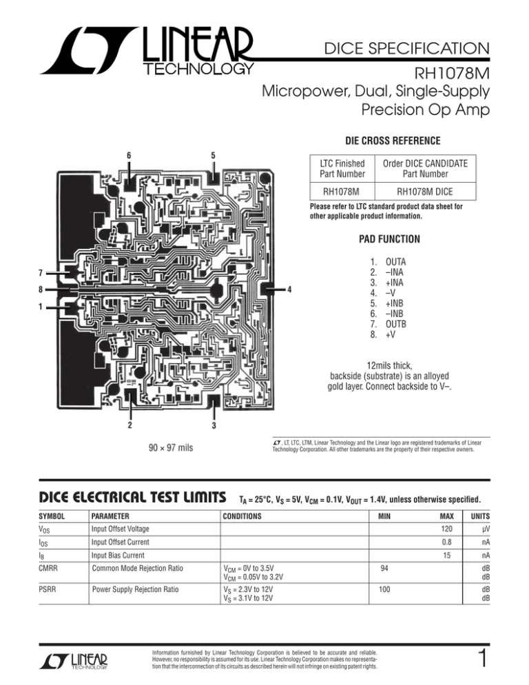
DICE SPECIFICATION RH1078M Micropower, Dual, Single-Supply Precision Op Amp DIE CROSS REFERENCE 6 5 LTC Finished Part Number Order DICE CANDIDATE Part Number RH1078M RH1078M DICE Please refer to LTC standard product data sheet for other applicable product information. PAD FUNCTION 7 8 4 1 1. 2. 3. 4. 5. 6. 7. 8. OUTA –INA +INA –V +INB –INB OUTB +V 12mils thick, backside (substrate) is an alloyed gold layer. Connect backside to V–. 2 3 L, LT, LTC, LTM, Linear Technology and the Linear logo are registered trademarks of Linear Technology Corporation. All other trademarks are the property of their respective owners. 90 × 97 mils DICE ELECTRICAL TEST LIMITS TA = 25°C, VS = 5V, VCM = 0.1V, VOUT = 1.4V, unless otherwise specified. SYMBOL PARAMETER MAX UNITS VOS Input Offset Voltage CONDITIONS 120 μV IOS Input Offset Current 0.8 nA IB Input Bias Current 15 nA CMRR Common Mode Rejection Ratio VCM = 0V to 3.5V VCM = 0.05V to 3.2V 94 dB dB PSRR Power Supply Rejection Ratio VS = 2.3V to 12V VS = 3.1V to 12V 100 dB dB Information furnished by Linear Technology Corporation is believed to be accurate and reliable. However, no responsibility is assumed for its use. Linear Technology Corporation makes no representation that the interconnection of its circuits as described herein will not infringe on existing patent rights. MIN 1 DICE SPECIFICATION RH1078M DICE ELECTRICAL TEST LIMITS TA = 25°C, VS = 5V, VCM = 0.1V, VOUT = 1.4V, unless otherwise specified. SYMBOL PARAMETER CONDITIONS MIN AVOL Large-Signal Voltage Gain VO = 0.03V to 4V, No Load VO = 0.03V to 3.5V, RL = 50k VO = 0.05V to 4V, No Load VO = 0.05V to 3.5V, RL = 50k 150 120 MAX UNITS VOUT Output Voltage Swing Output Low, No Load Output Low, 2k to GND Output Low, ISINK = 100μA Output High, No Load Output High, 2k to GND 4.2 3.5 mV mV mV V V 0.04 V/μs V/mV V/mV V/mV V/mV 6 2 130 SR Slew Rate A V = 1, VS = ±2.5V IS Supply Current Per Amplifier 75 μA Minimum Supply Voltage Note 2 2.3 V MAX UNITS TA = 25°C, VS = ±15V, unless otherwise specified. SYMBOL PARAMETER CONDITIONS MIN VOS Input Offset Voltage 350 μV IOS Input Offset Current 0.8 nA IB Input Bias Current 15 nA Input Voltage Range 13.5 –15.0 V V 97 dB dB CMRR Common Mode Rejection Ratio VCM = 13.5V, –15V VCM = 13V, –14.9V PSRR Power Supply Rejection Ratio VS = 5V, 0V to ±18V 100 dB AVOL Large-Signal Voltage Gain VO = ±10V, RL = 50k VO = ±10V, RL = 2k VO = ±10V, RL = 5k 1000 300 V/mV V/mV V/mV VOUT Output Voltage Swing RL = 50k RL = 2k RL = 5k ±13 ±11 V V V SR Slew Rate IS Supply Current 0.06 Per Amplifier Note 1: Stresses beyond those listed under Absolute Maximum Ratings may cause permanent damage to the device. Exposure to any Absolute Maximum Rating condition for extended periods may affect device reliability and lifetime. V/μs 100 μA Note 2: Power supply rejection ratio is measured at the minimum supply voltage. Wafer level testing is performed per the indicated specifications for dice. Considerable differences in performance can often be observed for dice versus packaged units due to the influences of packaging and assembly on certain devices and/or parameters. Please consult factory for more information on dice performance and lot qualifications via lot sampling test procedures. Dice data sheet subject to change. Please consult factory for current revision in production. I.D.No. 66-13-1078 2 Linear Technology Corporation LT 0314 REV B • PRINTED IN USA 1630 McCarthy Blvd., Milpitas, CA 95035-7417 (408) 432-1900 ● FAX: (408) 434-0507 ● www.linear.com LINEAR TECHNOLOGY CORPORATION 2005
