Soft-Switched PFC Boost Rectifier with Integrated ZVS Two
advertisement

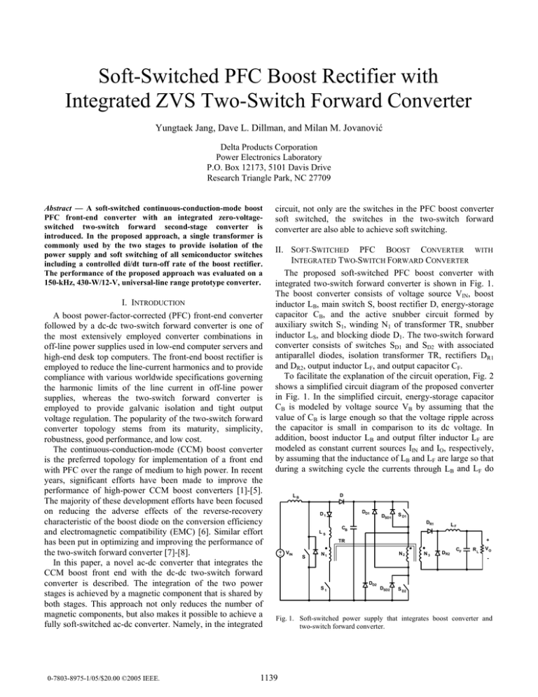
Soft-Switched PFC Boost Rectifier with Integrated ZVS Two-Switch Forward Converter Yungtaek Jang, Dave L. Dillman, and Milan M. Jovanović Delta Products Corporation Power Electronics Laboratory P.O. Box 12173, 5101 Davis Drive Research Triangle Park, NC 27709 Abstract — A soft-switched continuous-conduction-mode boost PFC front-end converter with an integrated zero-voltageswitched two-switch forward second-stage converter is introduced. In the proposed approach, a single transformer is commonly used by the two stages to provide isolation of the power supply and soft switching of all semiconductor switches including a controlled di/dt turn-off rate of the boost rectifier. The performance of the proposed approach was evaluated on a 150-kHz, 430-W/12-V, universal-line range prototype converter. I. INTRODUCTION A boost power-factor-corrected (PFC) front-end converter followed by a dc-dc two-switch forward converter is one of the most extensively employed converter combinations in off-line power supplies used in low-end computer servers and high-end desk top computers. The front-end boost rectifier is employed to reduce the line-current harmonics and to provide compliance with various worldwide specifications governing the harmonic limits of the line current in off-line power supplies, whereas the two-switch forward converter is employed to provide galvanic isolation and tight output voltage regulation. The popularity of the two-switch forward converter topology stems from its maturity, simplicity, robustness, good performance, and low cost. The continuous-conduction-mode (CCM) boost converter is the preferred topology for implementation of a front end with PFC over the range of medium to high power. In recent years, significant efforts have been made to improve the performance of high-power CCM boost converters [1]-[5]. The majority of these development efforts have been focused on reducing the adverse effects of the reverse-recovery characteristic of the boost diode on the conversion efficiency and electromagnetic compatibility (EMC) [6]. Similar effort has been put in optimizing and improving the performance of the two-switch forward converter [7]-[8]. In this paper, a novel ac-dc converter that integrates the CCM boost front end with the dc-dc two-switch forward converter is described. The integration of the two power stages is achieved by a magnetic component that is shared by both stages. This approach not only reduces the number of magnetic components, but also makes it possible to achieve a fully soft-switched ac-dc converter. Namely, in the integrated 0-7803-8975-1/05/$20.00 ©2005 IEEE. circuit, not only are the switches in the PFC boost converter soft switched, the switches in the two-switch forward converter are also able to achieve soft switching. II. SOFT-SWITCHED PFC BOOST CONVERTER WITH INTEGRATED TWO-SWITCH FORWARD CONVERTER The proposed soft-switched PFC boost converter with integrated two-switch forward converter is shown in Fig. 1. The boost converter consists of voltage source VIN, boost inductor LB, main switch S, boost rectifier D, energy-storage capacitor CB, and the active snubber circuit formed by auxiliary switch S1, winding N1 of transformer TR, snubber inductor LS, and blocking diode D1. The two-switch forward converter consists of switches SD1 and SD2 with associated antiparallel diodes, isolation transformer TR, rectifiers DR1 and DR2, output inductor LF, and output capacitor CF. To facilitate the explanation of the circuit operation, Fig. 2 shows a simplified circuit diagram of the proposed converter in Fig. 1. In the simplified circuit, energy-storage capacitor CB is modeled by voltage source VB by assuming that the value of CB is large enough so that the voltage ripple across the capacitor is small in comparison to its dc voltage. In addition, boost inductor LB and output filter inductor LF are modeled as constant current sources IIN and IO, respectively, by assuming that the inductance of LB and LF are large so that during a switching cycle the currents through LB and LF do D LB DD1 D1 LS DSD1 S D1 DR1 CB LF + TR VIN S N2 N1 S1 DD2 DSD2 N3 DR2 CF RL VO - S D2 Fig. 1. Soft-switched power supply that integrates boost converter and two-switch forward converter. 1139 - VD + D I IN iS i1 + VS - + V1 - DD1 iD D1 VB LS DSD1 i2 TR S S1 LM N1 n= + VS1 - S D1 + - N1 + V2 - N2 + VSD1 - DR1 i DR1 + N 3 V3 - i DR2 DR2 I O N2 DD2 DSD2 S D2 + VSD2 - Fig. 2. Simplified circuit diagram along with reference directions of key currents and voltages. not change significantly. In this analysis, the leakage inductance of the transformer is neglected because it does not have a significant effect on the operation of the circuit. Moreover, since snubber inductor LS and primary winding N1 of transformer TR are connected in series, the leakage inductance of the transformer is absorbed by LS. As a result, transformer TR is modeled by magnetizing inductance LM and the three-winding ideal transformer. Finally, it is assumed that in the on state, the semiconductors exhibit zero resistance, i.e., they are short circuits. However, the output capacitance of the switches, as well as the junction capacitance and the reverse-recovery charge of the boost rectifier are not neglected in this analysis. To further facilitate the analysis of operation, Fig. 3 shows the major topological stages of the circuit in Fig. 1 during a switching cycle, whereas Fig. 4 shows its key waveforms. The reference directions of currents and voltages plotted in Fig. 4 are shown in Fig. 2. As can be seen from the timing diagrams in Figs. 4(a), (b), and (c), the turn on of boost switch S and of forward switches SD1 and SD2 are synchronized, whereas auxiliary switch S1 is turned on prior to the turn on of switches S, SD1, and SD2. In addition, auxiliary switch S1 is turned off before boost switch S or forward switches SD1 and SD2 are turned off, i.e., the proposed circuit operates with overlapping gate drive signals for the active snubber switch and the converter switches. Prior to the turn on of switch S1 at t=T0, all switches are open. As a result, the entire input current IIN flows through boost rectifier D into energy-storage capacitor CB in the boost power stage, while output current IO flows through output rectifier DR2 in the two-switch forward power stage as shown in Fig. 3(j). Because output rectifier DR2 is conducting during this period, voltage v3 and induced voltage v1 across winding N1 of transformer TR is zero, i.e., v1=(N1/N3)v3=0. After switch S1 is turned on at t=T0, the voltage of energy-storagecapacitor VB is applied across snubber inductor LS so that current i1 starts to increase linearly, as illustrated in Fig. 4(g). The slope of current i1 is di1 VB . (1) = dt LS As current i1 starts flowing through winding N1 of transformer TR, the current in winding N3 also begins to increase, i.e., iDR1=(N1/N3)i1, as shown in Fig. 3(a) and Fig. 4(l). Because output current IO is constant and equal to the sum of rectifier currents iDR1 and iDR2, rectifier current iDR2 decreases until it becomes zero when rectifier current iDR1 increases. When rectifier current iDR2 becomes zero at t=T1, output rectifier DR2 turns off, as shown in Fig. 4(m). Since the current through winding N3 and rectifier DR1 is equal to output current IO after the turn-off of DR2, the increasing current in winding N1 makes current i2 in winding N2 begin to flow. This current discharges the output capacitances of forward switches SD1 and SD2, as illustrated in Fig. 3(b) and Fig. 4(i). During this period, voltage v2 across winding N2 of transformer TR starts to increase. After the output capacitances of forward switches SD1 and SD2 are fully discharged, switch currents iSD1 and iSD2 continue to flow through the antiparallel diodes of forward switches SD1 and SD2, as shown in Fig. 3(c) and Fig. 4(i). To achieve ZVS of forward switches SD1 and SD2, switches SD1 and SD2 should be turned on while their antiparallel diodes are conducting. To simplify the control circuit timing diagram, the turn-on of forward switches SD1 and SD2 is synchronized with the turnon of boost switch S. While the antiparallel diodes of forward switches SD1 and SD2 are conducting, voltage v2 across winding N2 is equal to VB so that induced voltage v1 on winding N1 is N v1 = 1 VB = nVB . (2) N2 Because v1 is constant, voltage applied across snubber inductor LS is also constant so that current i1 increases linearly with a slope of di1 VB − v1 VB − nVB V (3) = = = (1 − n ) B . dt LS LS LS During the same period, magnetizing inductance iM increases with a slope given by di M V (4) = B . dt LM As current i1 linearly increases, boost rectifier current iD linearly decreases at the same rate since the sum of i1 and iD is equal to constant input current IIN, i.e., i1+iD=IIN. Therefore, in the proposed circuit, the turn-off rate of the boost rectifier di D V (5) = −(1 − n ) B dt LS can be controlled by the proper selection of the inductance value of snubber inductor LS and turns ratio n of transformer TR. Typically, for today’s fast-recovery rectifiers, the turnoff rate diD/dt should be kept around 100 A/µs. With the selected turn-off rate, the reverse-recovery current of the 1140 iD i1 I IN + VS - + - VB + - i DR1 + V1 - + V2 - i DR2 IO VB i DR1 + V1 - I IN iS iM IO + VS1 - (a) [T0 - T1 ] (f) [T5 - T6 ] iD i1 I IN + VS - + - + - VB i DR1 + V1 - + V1 - I IN IO iM VB iM i DR2 IO + VS1 - iS (g) [T6 - T7 ] (b) [T1 - T2 ] iD i1 I IN + VS - + - + - VB i DR1 + V1 - IO iM I IN + VS - VB + V1 - iM i DR2 IO + VS1 - iS (h) [T7 - T8 ] (c) [T2 - T3 ] iD i1 + - + - VB i DR1 I IN IO iM I IN + VS - VB + V1 - iS IO iM i DR2 + VS1 - (i) [T8 - T9 ] (d) [T3 - T4 ] iD i1 + - i DR1 + V1 - I IN + - VB iM I IN IO + VS - VB + V1 - + V2 - + V3 - IO i DR2 + VS1 - iS (j) [T9 - T10 ] (e) [T4 - T5 ] Fig. 3. Topological stages. rectifier and the related power losses and EMI problems are minimized. After t=T2, current i1 starts to discharge the output capacitance of boost switch S and charge the junction capacitance of boost rectifier D, as shown in Fig. 3(c). If the turns ratio of transformer TR is selected so that n<0.5, the energy stored in LS is sufficient to completely discharge the output capacitance of boost switch S regardless of the load 1141 TS TON-PFC S1 t S t TON-DC-DC SD1 SD2 vSD1 vSD2 N1 N2 n= 2 t (1+n)VB vS1 (b) t (c) VB VB (a) (d) VB nVB vS t (e) VB i1 iS (1-n) VB LS - nVB LS VB LS t I IN (g) I IN nV B LS t t (h) i SD1 i SD2 VB LM iM - t VB LM t i D1 i D2 t i DR1 t i DR2 iD (f) t controlled di D dt = - (1-n) (j) (k) (l) (m) VB I IN LS t reverse-recovery charge vD (i) (n) VB T0T1 T T3T4 T5 2 T6 T7 T8 T9 T10 t (o) Fig. 4. Key waveforms. and line conditions. Once the capacitance is fully discharged at t=T3, current iS continues to flow through the antiparallel diode of boost switch S, as shown in Fig. 3(d) and Fig. 4(h). During this period, voltage v1 is applied in the negative direction across snubber inductor LS. Therefore, current i1 starts to decrease linearly at the rate given by di1 nV (6) =− B , dt LS as illustrated in Fig. 4(g). The current in auxiliary switch S1 also starts to decrease, whereas boost-switch current iS starts to increase from the negative peak value, as shown in Figs. 4(g) and (h). To achieve ZVS of boost switch S, it is necessary to turn on boost switch S before its current becomes positive at t=T4, i.e., during the period when current iS still flows through the antiparallel diode of switch S, as illustrated in Fig. 4(h). As shown in Fig. 4(g), current i1 continues to decrease until it reaches zero at t=T5. Shortly after t=T5, auxiliary switch S1 is turned off to achieve zero-current switching (ZCS). After switch S1 is turned off, the entire input current IIN flows through boost switch S. As a result, the front-end boost converter stage is completely decoupled from the twoswitch forward converter stage, as shown in Fig. 3(f). For the rest of the switching cycle, the two-switch forward converter stage continues to operate as a conventional two-switch forward converter. After forward switches SD1 and SD2 are turned off at t=T6, magnetizing current iM starts to charge the output capacitances of forward switches SD1 and SD2. When voltages vSD1 and vSD2 reach VB, the magnetizing current is diverted from forward switches SD1 and SD2 to clamp diodes DD1 and DD2, as shown in Fig. 3(g). At the same time, the reset of the transformer is initiated by bulk voltage VB applied across winding N2. During the reset time of the transformer, forward switch voltages vSD1 and vSD2 are equal to VO, whereas the voltage across auxiliary switch S1 is nVB due to the magnetic coupling of windings N1 and N2, as illustrated in Figs. 4(d) and (e). After boost switch S is turned off at t=T7, voltage across switch S starts to increase linearly because constant input current IIN begins charging the output capacitance of boost switch S, as shown in Fig. 3(h). The increasing boost-switch voltage causes an equal increase of voltage vS1 across auxiliary switch S1. When boost-switch voltage vS reaches VB at t=T8, boost diode D begins to conduct, as shown in Fig. 3(i). At the same time, auxiliary-switch voltage vS1 reaches its maximum value of (1+n)VB. The circuit stays in the topological stage shown in Fig. 3(i) until magnetizing current iM decreases to zero at t=T9. The next switching cycle is initiated at t=T10. In summary, the major feature of the proposed circuit in Fig. 1 is the soft-switching of all semiconductor devices. Specifically, boost switch S and forward switches SD1 and SD2 are turned on with ZVS, whereas auxiliary switch S1 is turned off with ZCS. In addition, boost diode D is turned off with a controlled turn-off rate of its current. Because all semiconductor components of the proposed converter operates with soft switching, the overall switching losses are minimized, which maximizes the conversion efficiency. In addition, soft switching has a beneficial effect on EMI and may result in a smaller size input filter [6]. However, it should be noted that complete ZVS of forward switches SD1 and SD2 can only be achieved if input current IIN is large enough to produce a negative current through primary winding N2 and discharge the output capacitances of switches SD1 and SD2 completely, as shown in Fig. 3(b). According to Fig. 3(b), to have a negative current flowing through winding N2 after t=T1, reflected current i1 into winding N3 has to be greater than output current IO. If this 1142 88 VGS1 [20 V/div] VGS [20 V/div] Efficiency [%] 86 84 i1 [10 A/div] ZCS 82 PROPOSED SOFT SWITCHING CONVERTER 80 VS [100 V/div] HARD SWITCHING CONVERTER ZVS 78 76 4 8 12 16 20 24 28 32 36 VGS1 [20 V/div] VGSD2 [20 V/div] Output Current [A] Fig. 5. Measured efficiency of 150 kHz, 430-W experimental converter with (dashed line) hard switching and (solid line) soft switching at VIN=90 VAC, VB=380 V, and VO=12 V as functions representing output current. controlled di/dt i1 [10 A/div] condition is not met, forward switches SD1 and SD2 operate with partial ZVS. This mode of operation typically occurs near the zero crossing of the line voltage in a PFC boost converter. Since the input current is proportional to the line voltage, input current IIN is small near the zero crossing of the line voltage. However, by adding an extra capacitor across boost switch S, forward switches SD1 and SD2 can achieve complete ZVS near the zero crossing of the line voltage. Due to the ZVS of boost switch S and forward switches SD1 and SD2, the most suitable switch component is a MOSFET (Metal Oxide Semiconductor Field Effect Transistor) device. Similarly, due to the ZCS of auxiliary switch S1, an IGBT (Insulated Gate Bipolar Transistor) is suitable for the auxiliary switch. In the proposed circuit, the voltage stresses on boost switch S, forward switches SD1 and SD2, and boost rectifier D are identical to the corresponding stresses in the conventional converters. However, the voltage stress of auxiliary switch S1 is (7) v S1( MAX) = (1 + n )VB . The control of the proposed circuit is performed by two independent controllers that are synchronized. Specifically, one controller is used to regulate the output voltage of the front-end boost stage, i.e., voltage VB across the energystorage capacitor CB. The other controller is used to regulate output voltage VO of the two-switch forward converter. III. EXPERIMENTAL RESULTS The performance of the proposed converter was evaluated on a 430-W prototype circuit that was designed to operate VSD2 [100 V/div] ZVS Fig. 6. Measured waveforms of experimental circuit at VIN=90 V, VB=380 V, IO= 26 A, VO=12 V. Time base: 1 µs/div. from a universal ac line input and deliver up to 36 A at 12 V output. Switches S, S1, SD1, and SD2 operate at 150 kHz. The experimental circuit was implemented with the following components: boost switch S and two-switch forward switches SD1 and SD2 – SPP20N60C2; auxiliary switch S1 – SPA11N80C3; boost diode D and snubber diode D1 – RHRP1560; output diodes DR1 and DR2 – S60SC6M; bulk capacitor CB – 470 uF/450 V; and output capacitor CF – 2 × 2200 uF/16 V. To build boost inductor LB, a toroidal core (MS130060) from Arnold and 71 turns of magnet wire (AWG #19) were used. External snubber inductor LS was connected in series with the auxiliary winding of transformer TR, as shown in Fig. 1. The required inductance is approximately 2.7 µH at full load. Snubber inductor LS was built using a toroidal core (A189043) and 9 turns of magnet wire (AWG #19). Transformer TR was built using a pair of ferrite cores (PJ403C94). Three magnet wires (N1=7 turns : N2=26 turns : N3=2 turns) were used. Figure 5 shows the measured efficiencies of the experimental converter with (solid lines) and without (dashed lines) the active snubber circuit as functions representing output current. As can be seen in Fig. 5, the active snubber 1143 V/36-A output. The proposed technique improves the efficiency by approximately 1.5% at full load. Input Voltage VIN VIN [50 V/div] IIN [5 A/div] REFERENCES Input current IIN Fig. 7. Measured waveforms of experimental circuit at VIN=90 V, VB=380 V, IO= 36 A, VO=12 V. Time base: 2 ms/div. improves the conversion efficiency in the entire measured power range. The active snubber improves the efficiency by approximately 1.5% at full load. Figures 6 and 7 show the oscillograms of key waveforms in the experimental converter. As can be seen from the corresponding waveforms in Fig. 4, there is a good agreement between the experimental and theoretical waveforms. As can be seen from Fig. 6, switches S and SD2 are turned on with ZVS since their voltages VS and VSD2 fall to zero before gate-drive signals VGS and VGSD2 become high. Moreover, auxiliary switch S1 achieves soft-switching turn off because switch current i1 becomes zero before auxiliary switch S1 is turned off. Also, it should be noted that the rising slope of current i1 is approximately di1/dt = 80 A/µs which is proportional to boost diode current iD during the period when boost diode D is turned off as shown in Fig. 6. The reverserecovery loss of boost diode D is dramatically reduced by the controlled diD/dt. Figure 7 shows the ac waveforms of input voltage VIN and input current IIN. The power factor of input current IIN is higher than 99%. [1] D.C. Martins, F.J.M. de Seixas, J.A. Brilhante, I. Barbi, “A family of dc-to-dc PWM converters using a new ZVS commutation cell,” IEEE Power Electronics Specialists' Conf. (PESC) Rec., pp. 524 - 530, June 1993. [2] G. Moschopoulos, P. Jain, G. Joós, “A novel zero-voltage switched PWM boost converter,” IEEE Power Electronics Specialists' Conf. (PESC) Rec., pp. 694-700, 1995. [3] J.-H. Kim, D.Y. Lee, H.S. Choi, B.H. Cho, “High performance boost PFP (power factor pre-regulator) with an improved ZVT (Zero Voltage Transition) converter,” IEEE Applied Power Electronics (APEC) Conf. Proc., pp. 337-342, 2001. [4] F.T. Wakabayashi, M.J. Bonato, C.A. Canesin, “Novel high-power factor ZCS-PWM preregulators,” IEEE Trans. Industrial Electronics, vol. 48, no. 2, pp. 322-333, Apr. 2001. [5] H.S. Choi, B.H. Cho, “Zero-current-switching (ZCS) power factor pre-regulator (pfp) with reduced conduction losses,” IEEE Applied Power Electronics (APEC) Conf. Proc., pp. 962 -967, 2002. [6] H. Chung, S.Y.R. Hui, K.K. Tse, “Reduction of Power Converter EMI Emission Using Soft-Switching Technique,” IEEE Trans. Electromagnetic Compatibility, vol. 40, no. 3, pp. 282-287, Aug. 1998. [7] A.P. Patel “Forward Converter Circuit Having Reduced Switching Losses,” US Patent 6,370,051B1, April 9, 2002. [8] G. Huang, Y. Gu, Z. Liu, and A.J. Zhang “Resonant Reset Dual Switch Forward Dc-to-Dc Converter,” US Patent 6,469,915B2, October 22, 2002. IV. SUMMARY A soft-switched boost PFC front-end converter with an integrated ZVS two-switch forward second-stage converter has been introduced. By using a single magnetic device which is mutually shared by the PFC boost converter and the two-switch forward converter, boost switch S and forward switches SD1 and SD2 are turned on with ZVS, auxiliary switch S1 is turned off with ZCS, and boost diode D is turned off softly using a controlled di/dt rate. As a result, the turn-on switching losses in the boost and forward switches, the turnoff switching loss in the auxiliary switch, and reverserecovery-related losses in the boost diode are eliminated, which maximizes the conversion efficiency. The performance of the proposed approach was evaluated on a 150-kHz, 430W, universal-line range prototype converter delivering 12- 1144


