A Novel EUV Phase Shift Mask Structure
C. Constancias1, M. Richard1, A.M. Nugrowati2, J-Y. Robic1
1. CEA - MINATEC -17 rue des Martyrs -38054 Grenoble, France
2. Optics Research Group, Technische Universiteit Delft, Lorentzweg 1, 2628CJ Delft, the Netherlands
christophe.constancias@cea.fr
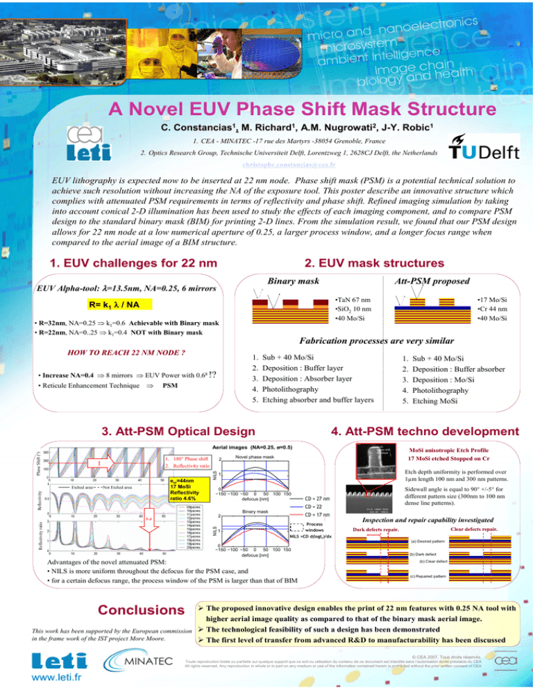
EUV lithography is expected now to be inserted at 22 nm node. Phase shift mask (PSM) is a potential technical solution to
achieve such resolution without increasing the NA of the exposure tool. This poster describe an innovative structure which
complies with attenuated PSM requirements in terms of reflectivity and phase shift. Refined imaging simulation by taking
into account conical 2-D illumination has been used to study the effects of each imaging component, and to compare PSM
design to the standard binary mask (BIM) for printing 2-D lines. From the simulation result, we found that our PSM design
allows for 22 nm node at a low numerical aperture of 0.25, a larger process window, and a longer focus range when
compared to the aerial image of a BIM structure.
2. EUV mask structures
1. EUV challenges for 22 nm
Binary mask
EUV Alpha-tool: λ=13.5nm, NA=0.25, 6 mirrors
Att-PSM proposed
•TaN 67 nm
•SiO2 10 nm
•40 Mo/Si
R= k1 λ / NA
• R=32nm, NA=0.25 ⇒ k1=0.6 Achievable with Binary mask
• R=22nm, NA=0..25 ⇒ k1=0.4 NOT with Binary mask
•17 Mo/Si
•Cr 44 nm
•40 Mo/Si
Fabrication processes are very similar
HOW TO REACH 22 NM NODE ?
1.
2.
3.
4.
5.
• Increase NA=0.4 ⇒ 8 mirrors ⇒ EUV Power with 0.68 !?
• Reticule Enhancement Technique ⇒
PSM
Sub + 40 Mo/Si
Deposition : Buffer layer
Deposition : Absorber layer
Photolithography
Etching absorber and buffer layers
1.
2.
3.
4.
5.
Sub + 40 Mo/Si
Deposition : Buffer absorber
Deposition : Mo/Si
Photolithography
Etching MoSi
200
7
3. Att-PSM Optical Design
4. Att-PSM techno development
1. 180° Phase shift
2. Reflectivity ratio
1
Not Etched area
Reflectivity
Etched area
ecr=44nm
17 MoSi
Reflectivity
ratio 4.6%
2
MoSi
Phase shift
multilayer
Novel phase mask
MoSi Blank multilayer
1
Binary mask
CD = 22 nm
CD = 15 nm
2
2
NILS
Process
windows
1
Etch depth uniformity is performed over
1µm length 100 nm and 300 nm patterns.
Sidewall angle is equal to 90° +/-5° for
different pattern size (300nm to 100 nm
dense line patterns).
0
−150 −100 −50 0 50 100 150
defocus [nm]
CD = 27 nm
σ = 0.5
NA = 0.25
Reflectivity ratio
MoSi anisotropic Etch Profile
17 MoSi etched Stopped on Cr
Chromium layer
NILS
Phase Shift (°)
Aerial images (NA=0.25, σ=0.5)
Inspection and repair capability investigated
Clear defects repair.
Dark defects repair.
NILS =CD d(logIx)/dx
(a) Desired pattern
0
−150 −100 −50 0 50 100 150
defocus [nm]
Advantages of the novel attenuated PSM:
• NILS is more uniform throughout the defocus for the PSM case, and
• for a certain defocus range, the process window of the PSM is larger than that of BIM
(b) Dark defect
(b) Clear defect
(c) Repaired pattern
Conclusions
The proposed innovative design enables the print of 22 nm features with 0.25 NA tool with
higher aerial image quality as compared to that of the binary mask aerial image.
The technological feasibility of such a design has been demonstrated
This work has been supported by the European commission
in the frame work of the IST project More Moore.
The first level of transfer from advanced R&D to manufacturability has been discussed
© CEA 2007. Tous droits réservés.
Toute reproduction totale ou partielle sur quelque support que ce soit ou utilisation du contenu de ce document est interdite sans l’autorisation écrite préalable du CEA
All rights reserved. Any reproduction in whole or in part on any medium or use of the information contained herein is prohibited without the prior written consent of CEA
www.leti.fr

