Midterm Solutions Physics 140B, Spring 2016
advertisement
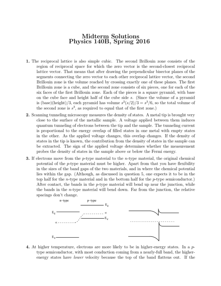
Midterm Solutions Physics 140B, Spring 2016 1. The reciprocal lattice is also simple cubic. The second Brillouin zone consists of the region of reciprocal space for which the zero vector is the second-closest reciprocal lattice vector. That means that after drawing the perpendicular bisector planes of the segments connecting the zero vector to each other reciprocal lattice vector, the second Brillouin zone is the volume reached by crossing exactly one of these planes. The first Brillouin zone is a cube, and the second zone consists of six pieces, one for each of the six faces of the first Brillouin zone. Each of the pieces is a square pyramid, with base on the cube face and height half of the cube side s. (Since the volume of a pyramid is (base)(height)/3, each pyramid has volume s2 (s/2)/3 = s3 /6, so the total volume of the second zone is s3 , as required to equal that of the first zone.) 2. Scanning tunneling microscopy measures the density of states. A metal tip is brought very close to the surface of the metallic sample. A voltage applied between them induces quantum tunneling of electrons between the tip and the sample. The tunneling current is proportional to the energy overlap of filled states in one metal with empty states in the other. As the applied voltage changes, this overlap changes. If the density of states in the tip is known, the contribution from the density of states in the sample can be extracted. The sign of the applied voltage determines whether the measurement probes the density of states in the sample above or below the Fermi energy. 3. If electrons move from the p-type material to the n-type material, the original chemical potential of the p-type material must be higher. Apart from that you have flexibility in the sizes of the band gaps of the two materials, and in where the chemical potential lies within the gap. (Although, as discussed in question 5, one expects it to be in the top half for the n-type material and in the bottom half for the p-type semiconductor.) After contact, the bands in the p-type material will bend up near the junction, while the bands in the n-type material will bend down. Far from the junction, the relative spacings don’t change. n−type p−type Ec Ec µ µ Ev Ev 4. At higher temperature, electrons are more likely to be in higher-energy states. In a ptype semiconductor, with most conduction coming from a nearly-full band, the higherenergy states have lower velocity because the top of the band flattens out. If the electrons at the hotter end move more slowly, then they will accummulate until the flux from the excess electrons at the hot end exactly balances the flux from the higher velocity electrons from the cold end. The charge imbalance creates an electric field directed towards the hot end, and a voltage that is higher at the cool end. 5. a) At zero temperature the chemical potential is in the middle of the gap. Two considerations shift its position at finite temperature: the asymmetry of the bands (i.e., a difference in effective masses), and the effect of dopants. Since dopants would move the chemical potential upward, closer to the conduction band, the band asymmetry, which can go in either direction, must dominate here. The conduction band must be much flatter (higher effective mass) than the valence band, as pictured. E k v b) Both contributions to the finite-temperature shift in µ are essentially linear: 34 kT ln m mc Nd and kT sinh−1 2n ≈ kT ln Nnid . (There is also temperature dependence in ni , i and Nd is only an approximation to the difference n − p, which is temperaturedependent, but at most temperatures these are lesser effects.) Typically Nd is several orders of magnitude larger than ni , while mc and mv rarely differ by more than one order of magnitude. Hence the second logarithm almost always dominates in actual semiconductors.
![Semiconductor Theory and LEDs []](http://s2.studylib.net/store/data/005344282_1-002e940341a06a118163153cc1e4e06f-300x300.png)
