Bessel Filter
advertisement

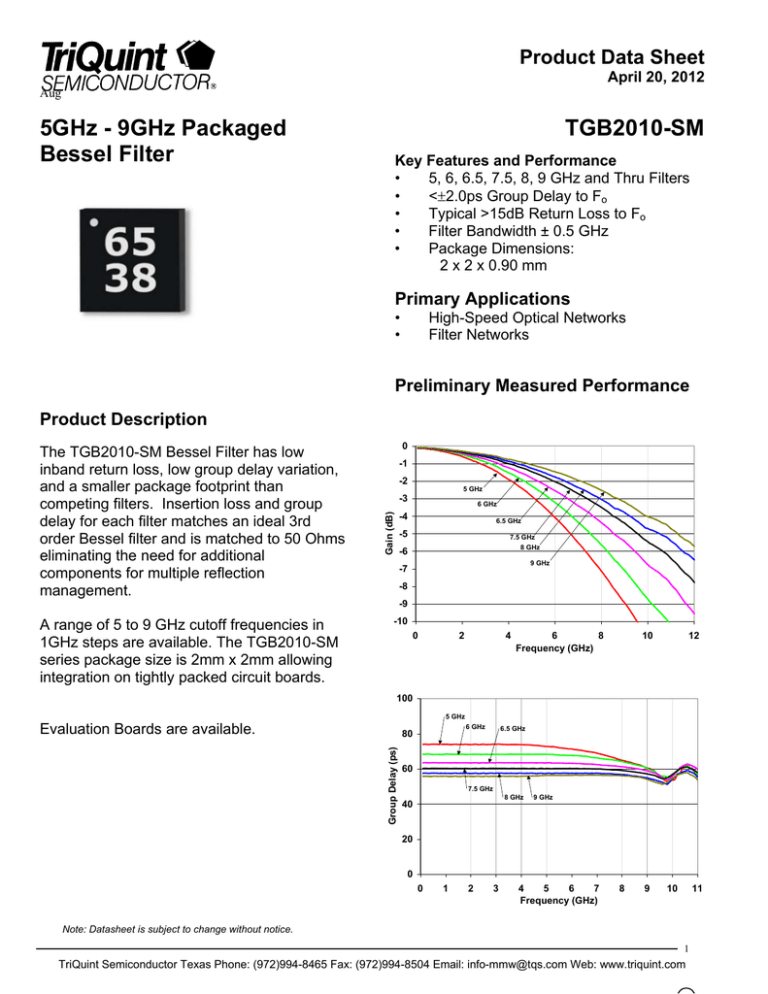
Product Data Sheet April 20, 2012 Aug 5GHz - 9GHz Packaged Bessel Filter TGB2010-SM Key Features and Performance • 5, 6, 6.5, 7.5, 8, 9 GHz and Thru Filters • <±2.0ps Group Delay to Fo • Typical >15dB Return Loss to Fo • Filter Bandwidth ± 0.5 GHz • Package Dimensions: 2 x 2 x 0.90 mm Primary Applications • • High-Speed Optical Networks Filter Networks Preliminary Measured Performance Product Description 0 -1 -2 5 GHz -3 Gain (dB) The TGB2010-SM Bessel Filter has low inband return loss, low group delay variation, and a smaller package footprint than competing filters. Insertion loss and group delay for each filter matches an ideal 3rd order Bessel filter and is matched to 50 Ohms eliminating the need for additional components for multiple reflection management. 6 GHz -4 6.5 GHz -5 7.5 GHz 8 GHz -6 9 GHz -7 -8 -9 A range of 5 to 9 GHz cutoff frequencies in 1GHz steps are available. The TGB2010-SM series package size is 2mm x 2mm allowing integration on tightly packed circuit boards. -10 0 2 4 6 8 Frequency (GHz) 12 10 100 5 GHz Evaluation Boards are available. 6 GHz Group Delay (ps) 80 6.5 GHz 60 7.5 GHz 8 GHz 40 9 GHz 20 0 0 1 2 3 4 5 6 7 Frequency (GHz) 8 9 10 11 Note: Datasheet is subject to change without notice. 1 TriQuint Semiconductor Texas Phone: (972)994-8465 Fax: (972)994-8504 Email: info-mmw@tqs.com Web: www.triquint.com Product Data Sheet April 20, 2012 TGB2010-SM TABLE I MAXIMUM RATINGS Symbol Parameter Value Notes PIN Input Continuous Wave Power in-band out-of-band 17 dBm 11 dBm TASSY Assembly Temperature 260 0C TSTG Storage Temperature -65 to 150 0C 1/ These ratings represent the maximum operable values for this device 1/ TABLE II TGB2010-SM RF CHARACTERIZATION TABLE (TA = 25°C, Nominal) Symbol Parameter Test Conditions Typical Units Fo 3dB Bandwidth (GHz) F = 5, 6, 6.5, 7.5, 8, 9 ±0.5 GHz Tg Group Delay Variation Within 3dB Bandwidth F=5-9 ±2.0 pS RL5GHz Return Loss F = DC - 5 GHz 15 dB RL6GHz Return Loss F = DC - 6 GHz 15 dB RL6.5GHz Return Loss F = DC - 6.5 GHz 15 dB RL7.5GHz Return Loss F = DC - 7.5 GHz 15 dB RL8GHz Return Loss F = DC - 7 GHz 15 dB RL9GHz Return Loss F = DC - 7 GHz 15 dB Notes Note: Table II Lists the RF Characteristics of typical devices as determined by fixtured measurements. 2 TriQuint Semiconductor Texas Phone: (972)994-8465 Fax: (972)994-8504 Email: info-mmw@tqs.com Web: www.triquint.com Product Data Sheet April 20, 2012 TGB2010-SM Measured Fixture Performance 0 -1 -2 Gain (dB) -3 -4 5 GHz 6 GHz 6.5 GHz 7.5 GHz 8 GHz 9 GHz -5 -6 -7 -8 -9 -10 0 2 4 6 8 Frequency (GHz) 10 12 0 Return Loss (dB) -5 -10 5 GHz 6 GHz 6.5 GHz 7.5 GHz 8 GHz 9 GHz -15 -20 -25 -30 0 1 2 3 4 5 6 7 8 Frequency (GHz) 9 10 11 12 3 TriQuint Semiconductor Texas Phone: (972)994-8465 Fax: (972)994-8504 Email: info-mmw@tqs.com Web: www.triquint.com Product Data Sheet April 20, 2012 TGB2010-SM Measured Fixture Performance 100 Group Delay (ps) 80 60 5 GHz 6 GHz 6.5 GHz 7.5 GHz 8 GHz 9 GHz 40 20 0 0 1 2 3 4 5 6 7 Frequency (GHz) 8 9 10 11 4 TriQuint Semiconductor Texas Phone: (972)994-8465 Fax: (972)994-8504 Email: info-mmw@tqs.com Web: www.triquint.com Product Data Sheet April 20, 2012 TGB2010-SM Package Pinout Pin 1 2 3 4 5 6 7 (Paddle) Signal NC Input NC NC Output NC Ground 5 TriQuint Semiconductor Texas Phone: (972)994-8465 Fax: (972)994-8504 Email: info-mmw@tqs.com Web: www.triquint.com Product Data Sheet April 20, 2012 TGB2010-SM Evaluation Board Input Output Note: No external components required. 6 TriQuint Semiconductor Texas Phone: (972)994-8465 Fax: (972)994-8504 Email: info-mmw@tqs.com Web: www.triquint.com Product Data Sheet April 20, 2012 TGB2010-SM Packaged Dimensional Drawing TGB2010-SM 7 TriQuint Semiconductor Texas Phone: (972)994-8465 Fax: (972)994-8504 Email: info-mmw@tqs.com Web: www.triquint.com Product Data Sheet April 20, 2012 TGB2010-SM Assembly of TGB2010-SM Surface Mount Package onto a Circuit Board Solders designated Pb-free such as SnAgCu have reflow temperatures which are higher than those required for Sn/Pb. Typical soldering temperatures are 20 to 30 degrees higher. The molding compound used in this package can withstand 260°C peak temperatures. In addition, the molding compound is free of flame retardants defined by some regulations as hazardous. 1. Clean the circuit board or module with Acetone. Rinse with alcohol and DI water. Allow the circuit to fully dry. 2. To improve the RF performance, we recommend attaching the paddle on the bottom of the package using Pb free solder. 3. Apply Pb free solder to each circuit board pad and to the backside contact for the package. 4. Reflow using manufacturer recommended oven and solder profiles. 5. Clean the assembly with alcohol. Ordering Information PACKAGE PART NUMBER DESIGNATIONS Part No Package Style Cutoff Frequency TGB2010-00-SM MLF/QFN Thru TGB2010-50-SM MLF/QFN 5.0 ± 0.5 GHz TGB2010-60-SM MLF/QFN 6.0 ± 0.5 GHz TGB2010-65-SM MLF/QFN 6.5 ± 0.5 GHz TGB2010-75-SM MLF/QFN 7.5 ± 0.5 GHz TGB2010-80-SM MLF/QFN 8.0 ± 0.5 GHz TGB2010-90-SM MLF/QFN 9.0 ± 0.5 GHz Note: Package marked with 2 digit center frequency and manufacturing week only. 8 TriQuint Semiconductor Texas Phone: (972)994-8465 Fax: (972)994-8504 Email: info-mmw@tqs.com Web: www.triquint.com


