THBT15011, THBT20011, THBT27011
Tripolar overvoltage protection for telecom line
Features
■
bidirectional crowbar protection between TIP
and GND, RING and GND and between TIP
and RING
■
peak pulse current:
IPP = 30 A for 10/1000 µs surge
■
holding current: IH = 150 mA
SO-8
Complies with Bellcore standard
■
TR-NWT-001089-Core, (second level) with line
series resistors:
– 10/1000 µs, 1000 V
– 2/10 µs, 2500 V (first level)
– 2/10 µs, 5000 V
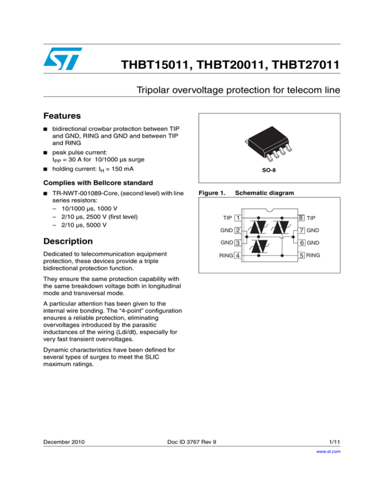
Figure 1.
Description
Dedicated to telecommunication equipment
protection, these devices provide a triple
bidirectional protection function.
Schematic diagram
TIP 1
8 TIP
GND 2
7 GND
GND 3
6 GND
RING 4
5 RING
They ensure the same protection capability with
the same breakdown voltage both in longitudinal
mode and transversal mode.
A particular attention has been given to the
internal wire bonding. The “4-point” configuration
ensures a reliable protection, eliminating
overvoltages introduced by the parasitic
inductances of the wiring (Ldi/dt), especially for
very fast transient overvoltages.
Dynamic characteristics have been defined for
several types of surges to meet the SLIC
maximum ratings.
December 2010
Doc ID 3767 Rev 9
1/11
www.st.com
11
Characteristics
1
THBT15011, THBT20011, THBT27011
Characteristics
Table 1.
Absolute maximum ratings (Tamb = 25 °C)
Symbol
Parameter
Value
Unit
Peak pulse current(1) (2)
10 / 1000 µs
30
A
ITSM
Non repetitive surge peak on-state current
(F = 50 Hz)
tp = 10 ms
t=1s
8
3.5
A
Tstg
Tj
Storage temperature range
Maximum junction temperature
- 40 to + 150
150
°C
260
°C
IPP
TL
Maximum lead temperature for soldering during 10s
1. For pulse waveform see Figure 2
2. See Figure 7: Test circuit 4 for IPP parameter
Figure 2.
Pulse waveform
% I
PP
Repetitive peak pulse current
10 0
tr = rise time (µs)
tp = pulse duration time (µs)
50
0
tr
Figure 3.
t
tp
Surge peak current versus overload duration
ITSM(A)
10
F=50Hz
Tj initial=25°C
9
8
7
6
5
4
3
2
1
t(s)
0
1E-2
Table 2.
2/11
1E+0
1E+1
1E+2
1E+3
Thermal resistance
Symbol
Rth(j-a)
1E-1
Parameter
Junction to ambient
Doc ID 3767 Rev 9
Value
Unit
170
°C/W
THBT15011, THBT20011, THBT27011
Table 3.
Characteristics
Electrical characteristics (Tamb = 25 °C)
Symbol
Parameter
I
IPP
VRM
Stand-off voltage
IRM
Leakage current at stand-off voltage
VR
Continuos reverse voltage
VBR
Breakdown voltage
VBO
Breakover voltage
IH
Holding current
IBO
Breakover current
VF
Forward voltage drop
IPP
Peak pulse current
C
Table 4.
IBO
IH
V
IR
VRM VBR VBO
Capacitance
Static parameters
IR(1) @ VR
IRM @ VRM
Order code
max.
max.
VBO(2) @ IBO
IH(3)
C(4)
max.
min.
max.
min.
max.
µA
V
µA
V
V
V
mA
mA
pF
THBT15011D
5
135
50
150
210
50
400
150
80
THBT20011D
5
180
50
200
290
50
400
150
80
THBT27011D
5
240
50
270
380
50
400
150
80
1. IR measured at VR guarantee VBR min ≥ VR
2. Measured at 50 Hz (1 cycle) - See Figure 4: Test circuit 1 for IBO and VBO parameters.
3. See Figure 5: Test circuit 2 for dynamic IH parameter.
4. VR = 1 V, F = 1 MHz.
Table 5.
Dynamic breakover voltages (transversal mode)
Type
Test conditions(1)
Symbol
Max
Unit
1.5 kV
1.5 kV
2.5 kV
Rp = 10 Ω
Rp = 10 Ω
Rp = 62 Ω
IPP = 30 A
IPP = 30 A
IPP = 38 A
190
190
200
V
THBT15011D
VBO
10/700 µs
1.2/50 µs
2/10μs
THBT20011D
VBO
10/700 µs
1.2/50 µs
2/10 µs
1.5 kV
1.5 kV
2.5 kV
Rp = 10 Ω
Rp = 10 Ω
Rp = 62 Ω
IPP = 30 A
IPP = 30 A
IPP = 38 A
270
270
280
V
THBT27011D
VBO
10/700 µs
1.2/50 µs
2/10 µs
1.5 kV
1.5 kV
2.5 kV
Rp = 10 Ω
Rp = 10 Ω
Rp = 62 Ω
IPP = 30 A
IPP = 30 A
IPP = 38 A
360
360
400
V
1. See Figure 6: Test circuit 3 for VBO parameters. Rp is the protection resistor located on the line card.
Doc ID 3767 Rev 9
3/11
Test circuits
THBT15011, THBT20011, THBT27011
2
Test circuits
2.1
Test procedure for test circuit 1 for IBO and VBO parameters
Figure 4.
Test circuit 1 for IBO and VBO parameters
K
ton = 20ms
R1 = 140Ω
R2 = 240Ω
220V 50Hz
DUT
Vout
VBO
measurement
1/4
IBO
measurement
Pulse test duration (tp = 20 ms):
●
For bidirectional devices switch K is closed.
●
For unidirectional devices switch K is open.
VOUT selection:
2.2
●
For device with VBO < 200 V, VOUT = 250 VRMS, R1 = 140 Ω.
●
For device with VBO ≥ 200 V, VOUT = 480 VRMS, R2 = 240 Ω.
Test procedure for test circuit 2 for dynamic IH parameter
Figure 5.
Test circuit 2 for dynamic IH parameter
R
Surge generator
D.U.T
VBAT = - 48 V
This is a go no-go test, which can confirm the holding current (IH) level.
Procedure
4/11
1.
Adjust the current level at the IH value by short circuiting the AK of the D.U.T.
2.
Fire the D.U.T. with a surge current IPP = 10A, 10/1000µs.
3.
The D.U.T. will come back off-state within 50 ms maximum.
Doc ID 3767 Rev 9
THBT15011, THBT20011, THBT27011
2.3
Test circuits
Test circuit 3 for VBO parameters
Figure 6.
Test circuit 3 for VBO parameters
R4
(V P is defined in no load condition)
L
T IP
R2
R IN G
R3
VP
R1
C1
C2
G ND
Table 6.
Parameters for test crcuit 3 for selected pulse characteristics
Pulse (µs)
2.4
Vp
(V)
C1
(µF)
C2
(nF)
L
(µH)
R1
(Ω)
R2
(Ω)
R3
(Ω)
R4
(Ω)
IPP
(A)
Rp
(Ω)
tr
tp
10
700
1500
20
200
0
50
15
25
25
30
10
1.2
50
1500
1
33
0
76
13
25
25
30
10
2
10
2500
10
0
1.1
1.3
0
3
3
38
62
Test circuit 4 for IPP parameter
Figure 7.
Test circuit 4 for IPP parameter
Longitudinal mode
TIP
See test
circuit 3
IPP/2
RP
IPP/2
RP
RING
THBT
GND
Transversal mode
TIP or
RING I
PP
RP
THBT
See test
circuit 3
GND
Doc ID 3767 Rev 9
5/11
Application information
3
THBT15011, THBT20011, THBT27011
Application information
Figure 8.
Device connections
TIP 1
8 TIP
2
7
GND
GND
3
6
RING 4
5 RING
Connect pins 2, 3, 6 and 7 to ground to guarantee a good surge current capability for long
duration disturbances.
To take advantage of the “4-point” structure of the THBT, the TIP and RING lines have to
cross the device. In this case, the device will eliminate the overvoltages generated by the
parasitic inductances of the wiring (Ldi/dt), especially for very fast transients.
3.1
Application circuits
Figure 9.
Line card protection
RING
GENERATOR
- VBAT
PTC
LINE A
T
E
S
T
RING
RELAY
R
SLIC
E
L
220
nF
A
Y
S
LINE B
6/11
THBTxxxD
LCP1511D
PTC
Doc ID 3767 Rev 9
THBT15011, THBT20011, THBT27011
Application information
Figure 10. Protection for telephone set with ground key
Hook
LA
Speech
dialing
ringer
LB
THBTxxxD
Ground key
E
Doc ID 3767 Rev 9
7/11
Ordering information scheme
4
THBT15011, THBT20011, THBT27011
Ordering information scheme
Figure 11. Ordering information scheme
THBT 150 1 1 D RL
Bidirectional Trisil™
Breakdown voltage
Version
Package
1 = SO-8 plastic
Dynamic
Packing
(Blank) = Tube
RL = Tape and reel
TM: Transil is a trademark of STMicroelectronics
8/11
Doc ID 3767 Rev 9
THBT15011, THBT20011, THBT27011
5
Package information
Package information
●
Epoxy meets UL94, V0
●
Lead-free package
In order to meet environmental requirements, ST offers these devices in different grades of
ECOPACK® packages, depending on their level of environmental compliance. ECOPACK®
specifications, grade definitions and product status are available at: www.st.com.
ECOPACK® is an ST trademark.
Table 7.
SO-8 dimensions
Dimensions
Ref.
Min.
Seating
Plane
C
A2
A
L
k
ppp C
L1
D
8
5
E1
1
Typ.
Inches
Max.
Min.
Typ.
Max.
h x 45°
C
A1
e
b
A
Millimeters
E
1.75
A1
0.1
A2
1.25
b
0.25
0.004
0.28
0.48
0.011
0.019
C
0.17
0.23
0.007
0.009
D
4.80
5.00
0.189 0.193 0.197
0.049
4.90
E
5.80
6.00
6.20
0.228 0.236 0.244
3.80
3.90
4.00
0.150 0.154 0.157
1.27
h
0.25
L
0.40
L1
0.050
0.50
0.010
1.27
0.016
1.04
k
0°
ppp
Figure 12. Footprint, dimensions in mm
(inches)
0.010
E1
e
4
0.069
0.020
0.050
0.041
8°
0°
0.10
8°
0.004
Figure 13. Marking
6.8
(0.268)
0.6
(0.024)
x x x x x x
4.2
(0.165)
®
z z y ww
XXXXX : Marking
ZZ : Manufacturing
Y : Year
WW : week
location
1.27
(0.050)
Pin 1
Doc ID 3767 Rev 9
9/11
Ordering information
6
THBT15011, THBT20011, THBT27011
Ordering information
Table 8.
Ordering information
Order code
7
THBT15011D
BT151D
THBT20011D
BT201D
THBT27011D
BT271D
Package
Weight
SO-8
0.077 g
Revision history
Table 9.
10/11
Marking
Document revision history
Date
Revision
Changes
Oct-2003
7A
19-Feb-2008
8
Reformatted to current standards. Removed THBT16011D from Table 4
and Table 8. Updated Figure 4, Figure 5, and Figure 9. Added ECOPACK
paragraph in Section 5. Added Figure 13: Marking.
09-Dec-2010
9
Restructured for conformity with other products in this class. Updated
trademark statement for Trisil in Figure 11.
Previous release
Doc ID 3767 Rev 9
THBT15011, THBT20011, THBT27011
Please Read Carefully:
Information in this document is provided solely in connection with ST products. STMicroelectronics NV and its subsidiaries (“ST”) reserve the
right to make changes, corrections, modifications or improvements, to this document, and the products and services described herein at any
time, without notice.
All ST products are sold pursuant to ST’s terms and conditions of sale.
Purchasers are solely responsible for the choice, selection and use of the ST products and services described herein, and ST assumes no
liability whatsoever relating to the choice, selection or use of the ST products and services described herein.
No license, express or implied, by estoppel or otherwise, to any intellectual property rights is granted under this document. If any part of this
document refers to any third party products or services it shall not be deemed a license grant by ST for the use of such third party products
or services, or any intellectual property contained therein or considered as a warranty covering the use in any manner whatsoever of such
third party products or services or any intellectual property contained therein.
UNLESS OTHERWISE SET FORTH IN ST’S TERMS AND CONDITIONS OF SALE ST DISCLAIMS ANY EXPRESS OR IMPLIED
WARRANTY WITH RESPECT TO THE USE AND/OR SALE OF ST PRODUCTS INCLUDING WITHOUT LIMITATION IMPLIED
WARRANTIES OF MERCHANTABILITY, FITNESS FOR A PARTICULAR PURPOSE (AND THEIR EQUIVALENTS UNDER THE LAWS
OF ANY JURISDICTION), OR INFRINGEMENT OF ANY PATENT, COPYRIGHT OR OTHER INTELLECTUAL PROPERTY RIGHT.
UNLESS EXPRESSLY APPROVED IN WRITING BY AN AUTHORIZED ST REPRESENTATIVE, ST PRODUCTS ARE NOT
RECOMMENDED, AUTHORIZED OR WARRANTED FOR USE IN MILITARY, AIR CRAFT, SPACE, LIFE SAVING, OR LIFE SUSTAINING
APPLICATIONS, NOR IN PRODUCTS OR SYSTEMS WHERE FAILURE OR MALFUNCTION MAY RESULT IN PERSONAL INJURY,
DEATH, OR SEVERE PROPERTY OR ENVIRONMENTAL DAMAGE. ST PRODUCTS WHICH ARE NOT SPECIFIED AS "AUTOMOTIVE
GRADE" MAY ONLY BE USED IN AUTOMOTIVE APPLICATIONS AT USER’S OWN RISK.
Resale of ST products with provisions different from the statements and/or technical features set forth in this document shall immediately void
any warranty granted by ST for the ST product or service described herein and shall not create or extend in any manner whatsoever, any
liability of ST.
ST and the ST logo are trademarks or registered trademarks of ST in various countries.
Information in this document supersedes and replaces all information previously supplied.
The ST logo is a registered trademark of STMicroelectronics. All other names are the property of their respective owners.
© 2010 STMicroelectronics - All rights reserved
STMicroelectronics group of companies
Australia - Belgium - Brazil - Canada - China - Czech Republic - Finland - France - Germany - Hong Kong - India - Israel - Italy - Japan Malaysia - Malta - Morocco - Philippines - Singapore - Spain - Sweden - Switzerland - United Kingdom - United States of America
www.st.com
Doc ID 3767 Rev 9
11/11
