Counter Design: Synchronous & Asynchronous Circuits
advertisement

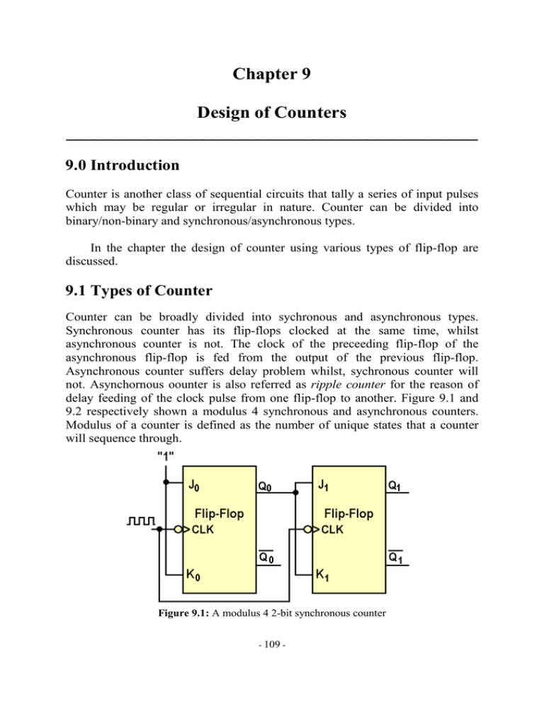
Chapter 9 Design of Counters _____________________________________________ 9.0 Introduction Counter is another class of sequential circuits that tally a series of input pulses which may be regular or irregular in nature. Counter can be divided into binary/non-binary and synchronous/asynchronous types. In the chapter the design of counter using various types of flip-flop are discussed. 9.1 Types of Counter Counter can be broadly divided into sychronous and asynchronous types. Synchronous counter has its flip-flops clocked at the same time, whilst asynchronous counter is not. The clock of the preceeding flip-flop of the asynchronous flip-flop is fed from the output of the previous flip-flop. Asynchronous counter suffers delay problem whilst, sychronous counter will not. Asynchornous oounter is also referred as ripple counter for the reason of delay feeding of the clock pulse from one flip-flop to another. Figure 9.1 and 9.2 respectively shown a modulus 4 synchronous and asynchronous counters. Modulus of a counter is defined as the number of unique states that a counter will sequence through. Figure 9.1: A modulus 4 2-bit synchronous counter - 109 - 09 Design of Counters Figure 9.2: A modulus 4 2-bit asynchrounous counter 9.2 Propagation Delay We have mentioned in earlier in Chapter one that there is propagation delay when data is transmitted from one device to another due to capacitance of the device. The problem associated with propagation delay can be serious. We shall illustrate propagation delay with a 3-bit binary counter and its timing diagram shown in Fig. 9.3 and 9.4 respectively. Figure 9.3: 3-bit (modulus 8) binary counter - 110 - 09 Design of Counters Figure 9.4: The actual timing diagram of a 3-bit binary counter From the timing diagram, it shows there are propagation delays due to transition from clock pulse to output of flip-flop 0 Q0, from output of flip-flop 0 Q0 to output flip-flop 1 Q1, and from output of flip-flop 1 Q1 to output flip-flop 2 Q2. If the output Q1 is AND’ed with output Q 0 , the ideal result i.e. the assumption of no propagation delay is shown in Fig. 9.5, whereas the result shown in Fig. 9.6 is different for the case where there is propagation delay. There are glitches for the non-ideal case. Figure 9.5: Ideal result of Q1• Q 0 - 111 - 09 Design of Counters Figure 9.6: Non-ideal result of Q1• Q 0 In reality, the propagation is in the nanosecond region, which is not as large as it shown in the figure. It is about 10ns for each type. 9.3 Procedure to Design Synchronous Counters The procedure to design a synchronous counter is listed here. • Obtain the truth table of the logic sequence for intended counter to be designed. Alternatively obtain the state diagram of the counter. • Determine the number and type of flip-flop to be used. • From the excitation table of the flip-flop, determine the next state logic. • From the output state, use Karnaugh map for simplification to derive the circuit output functions and the flip-flop output functions. • Draw the logic circuit diagram. • Simulate the circuit using software. • Build the circuit. From the function tables shown in Fig. 7.4, 7.10, 7.17, and 7.20 of the flip-flops learnt earlier in Chapter 7, the excitation or characteristic table of SR flip-flop, D flip-flip, JK flip-flop, and T flip-flop are shown in Fig. 9.7. and 9.8 respectively. Qt is denotes the output of the present state and Qt+1 denotes the output of next state. - 112 - 09 Design of Counters Qt 0 0 1 1 Qt+1 0 1 0 1 S 0 1 0 X R X 0 1 0 Qt 0 0 1 1 Qt+1 0 1 0 1 D 0 1 0 1 Figure 9.7: Characteristic table of SR and D flip-flop Qt 0 0 1 1 Qt+1 0 1 0 1 J 0 1 X X K X X 1 0 Qt 0 0 1 1 Qt+1 0 1 0 1 T 0 1 1 0 Figure 9.8: Characteristic table of JK and T flip-flop 9.4 Design of Synchronous Counters In this section, designing of various types of synchronous counter using different types of flip-flop are discussed. Using the procedure and function tables mentioned in section 9.2, a step by step ways to design the synchronous counter discussed. 9.4.1 Design of a Synchronous Decade Counter Using JK FlipFlop A synchronous decade counter will count from zero to nine and repeat the sequence. The state diagram of this counter is shown in Fig. 9.9. Figure 9.9: State diagram of synchronous decde counter - 113 - 09 Design of Counters Since there are ten states, four JK flip-flops are required. The truth tables of present and next state for the decade counter are shown in Fig. 9.10. Using the excitation table of JK flip-flop and the outputs of J and K are filled. Present State Q3 Q2 Q1 Q0 0 0 0 0 0 0 0 1 0 0 1 0 0 0 1 1 0 1 0 0 0 1 0 1 0 1 1 0 0 1 1 1 1 0 0 0 1 0 0 1 Q3 0 0 0 0 0 0 0 1 1 0 Next State Q2 Q1 0 0 0 1 0 1 1 0 1 0 1 1 1 1 0 0 0 0 0 0 Q0 1 0 1 0 1 0 1 0 1 0 J3 K3 0 X 0 X 0 X 0 X 0 X 0 X 0 X 1 X X 0 X 1 J2 0 0 0 1 X X X X 0 0 Output K2 J1 X 0 X 1 X X X X 0 0 0 1 0 X 1 X X 0 X 0 K1 X X 0 1 X X 0 1 X X J0 K0 1 X X 1 1 X X 1 1 X X 1 1 X X 1 1 X X 1 Figure 9.10: Truth table and state table of a synchronous decade counter The Karnaugh maps of the output J0, K0, J1, K1, J2, K2, J3, and K3 are shown in Fig. 9.11, 9.12, 9.13, and 9.14 respectively. The simplified results are at the bottom of the Karnaugh maps. Figure 9.11: Karnaugh maps of J0 and K0 - 114 - 09 Design of Counters Figure 9.12: Karnaugh maps of J1 and K1 Figure 9.13: Karnaugh maps of J2 and K2 Figure 9.14: Karnaugh maps of J3 and K3 - 115 - 09 Design of Counters Based on the results obtained from the Karnaugh maps, the circuit design of synchronous decade counter is shown in Fig. 9.15. Figure 9.15: A synchronous decade counter designed using JK flip-flop 9.4.2 Design of an Asynchronous Decade Counter Using JK FlipFlop An asynchronous decade counter will count from zero to nine and repeat the sequence. Since the JK inputs are fed fom the output of previous flip-flop, therefore, the design will not be as complicated as the syncrhonous version. At the nineth count, the counter is reset to begin counting at zero. The NAND gate is used to reset the counter at the ninth count. At the ninth count the outputs of flip-flop Q3 and Q1 will be high simultaneously. This will cause the output of NAND to go to logic “0” that would reset the flip-flip. The logic design of the counter is shown in Fig. 9.16. Figure 9.16: An asynchronous decade counter - 116 - 09 Design of Counters 9.4.3 Design of a Synchronous Modulus-Six Counter Using SR Flip-Flop The modulus six counter will count 0, 2, 3, 6, 5, and 1 and repeat the sequence. This modulus six counter requires three SR flip-flops for the design. The truth table of a modulus six counter is shown in Fig. 9.17. From the excitation table of SR flip-flop shown in Fig. 9.8, the logic of output S2, R2, S1, R1, S0, and R0 are filled and shown in Fig. 9.8. [Present State Next State Q2 Q1 Q0 Q2 Q1 Q0 0 0 0 0 1 0 0 1 0 0 1 1 0 1 1 1 1 0 1 1 0 1 0 1 1 0 1 0 0 1 0 0 1 0 0 0 R2 0 0 1 X 0 0 S2 X X 0 0 1 X Output R1 S1 1 0 X 0 X 0 0 1 0 X 0 X R0 S0 0 X 1 0 0 1 1 0 X 0 0 1 Figure 9.17: Truth table and state table of the modulus-six counter The state diagram is shown in Fig. 9.18. Figure 9.18: State diagram of modulus-six counter - 117 - 09 Design of Counters The Karnaugh maps of the output R0, S0, R1, S1, R2, and S2 are shown in Fig. 9.19, 9.20, and 9.21 respectively. The simplified results are at the bottom of the Karnaugh maps. Figure 9.19: Karnaugh maps of R0 and S0 Figure 9.20: Karnaugh maps of R1 and S1 Figure 9.21: Karnaugh maps of R2 and S2 With the known output logic functions, the logic design of the synchronous modulus six counter is hown ing Fig. 9.21. - 118 - 09 Design of Counters Figure 9.22: Logic design of synchronous modulus six counters - 119 - 09 Design of Counters Tutorials 9.1. State the procedure for design a synchronous counter. 9.2. Draw the timing diagrams of the decade counter shown in Fig. 9.14. 9.3. Design a modulus seven synchronous counter that can count 0, 3, 5, 7, 9, 11, and 12 using D flip-flop. 9.4. Using the truth table shown in Fig. 9.16, design this counter using T flipflop. References 1. Thomas L. Floyd, "Digital Fundamentals", Seventh Edition, Prentice-Hall International, Inc., 2000. 2. Donald D. Givone, "Digital Principles and Designs", McGraw- Hill 2003. 3. Victor P. Nelson, H. Try Nagle, Bill D. Carroll, and J. David Irwin, "Digital Logic Circuit Analysis & Design", Prentice-Hall Englewood Cliffs.NJ, 1995. - 120 -

