Designing with FPGAs Compared with SSI/MSI Devices
advertisement

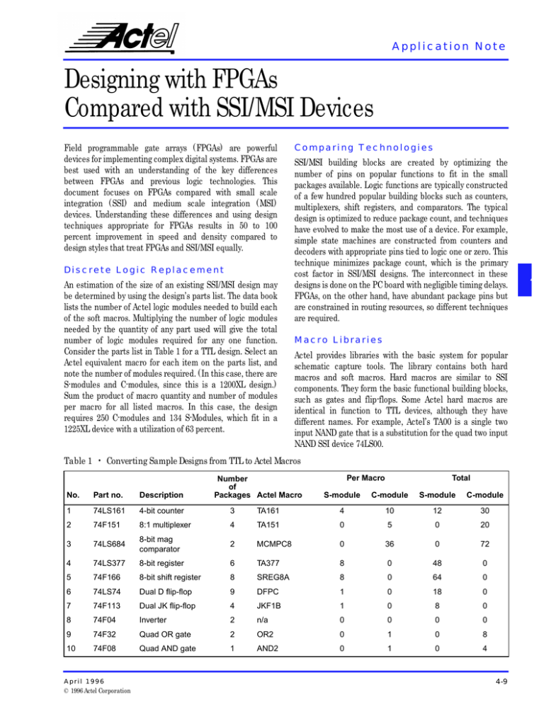
Appl i cat i on N ot e Designing with FPGAs Compared with SSI/MSI Devices Field programmable gate arrays (FPGAs) are powerful devices for implementing complex digital systems. FPGAs are best used with an understanding of the key differences between FPGAs and previous logic technologies. This document focuses on FPGAs compared with small scale integration (SSI) and medium scale integration (MSI) devices. Understanding these differences and using design techniques appropriate for FPGAs results in 50 to 100 percent improvement in speed and density compared to design styles that treat FPGAs and SSI/MSI equally. Discrete Logic Replacement An estimation of the size of an existing SSI/MSI design may be determined by using the design’s parts list. The data book lists the number of Actel logic modules needed to build each of the soft macros. Multiplying the number of logic modules needed by the quantity of any part used will give the total number of logic modules required for any one function. Consider the parts list in Table 1 for a TTL design. Select an Actel equivalent macro for each item on the parts list, and note the number of modules required. (In this case, there are S-modules and C-modules, since this is a 1200XL design.) Sum the product of macro quantity and number of modules per macro for all listed macros. In this case, the design requires 250 C-modules and 134 S-Modules, which fit in a 1225XL device with a utilization of 63 percent. Comparing Technologies SSI/MSI building blocks are created by optimizing the number of pins on popular functions to fit in the small packages available. Logic functions are typically constructed of a few hundred popular building blocks such as counters, multiplexers, shift registers, and comparators. The typical design is optimized to reduce package count, and techniques have evolved to make the most use of a device. For example, simple state machines are constructed from counters and decoders with appropriate pins tied to logic one or zero. This technique minimizes package count, which is the primary cost factor in SSI/MSI designs. The interconnect in these designs is done on the PC board with negligible timing delays. FPGAs, on the other hand, have abundant package pins but are constrained in routing resources, so different techniques are required. Macro Libraries Actel provides libraries with the basic system for popular schematic capture tools. The library contains both hard macros and soft macros. Hard macros are similar to SSI components. They form the basic functional building blocks, such as gates and flip-flops. Some Actel hard macros are identical in function to TTL devices, although they have different names. For example, Actel’s TA00 is a single two input NAND gate that is a substitution for the quad two input NAND SSI device 74LS00. Table 1 • Converting Sample Designs from TTL to Actel Macros Number of Packages Actel Macro No. Part no. Description 1 74LS161 4-bit counter 3 2 74F151 8:1 multiplexer 3 74LS684 4 Per Macro Total S-module C-module S-module C-module TA161 4 10 12 30 4 TA151 0 5 0 20 8-bit mag comparator 2 MCMPC8 0 36 0 72 74LS377 8-bit register 6 TA377 8 0 48 0 5 74F166 8-bit shift register 8 SREG8A 8 0 64 0 6 74LS74 Dual D flip-flop 9 DFPC 1 0 18 0 7 74F113 Dual JK flip-flop 4 JKF1B 1 0 8 0 8 74F04 Inverter 2 n/a 0 0 0 0 9 74F32 Quad OR gate 2 OR2 0 1 0 8 10 74F08 Quad AND gate 1 AND2 0 1 0 4 April 1996 © 1996 Actel Corporation 4-9 4 Soft macros are more complex functions built from a number of hard macros. Some soft macro examples are counters, decoders, and adders. All soft macros are easily copied, modified, and saved in user libraries. Should you need an SSI/MSI function for which there is no equivalent in the library, it is easy to build it by creating the schematic from a TTL manual, using the Actel library. The Actel FPGA Macro Library Guide contains complete information on all the Actel library components, including a specific TTL section. If you do not require all the outputs of a soft macro, you do not have to modify the macro. The Actel combiner program (invoked during compile) will automatically eliminate any unused modules before the design is placed and routed. All macro inputs, however, must be connected to another module output, VCC, or ground. For optimal module usage, it is best to copy the macro and the underlying schematic and then edit both of these to reflect the logic reduction. Three-State Implementation Many SSI/MSI devices have three-state outputs allowing them to be connected to a common bus. The three-state function should be implemented with a multiplexer, which is particularly effective in an Actel FPGA. Figure 1 shows a three-state SSI/MSI implementation as well as the FPGA multiplexer implementation. An 8-bit bus with four possible drivers can be implemented with only eight logic modules, or less than 3 percent of an Actel A1010 device. State Machine Techniques A common state machine design technique with MSI devices uses a loadable counter to implement a state machine. Load inputs are tied to a jump address. (Sometimes logic is used if more than one jump address is needed.) The counter either counts (to advance to the next state) or loads (to jump to a different state). This is efficient in MSI devices, since it requires only a couple of packages to implement a simple state machine. Although this design technique reduces MSI package count, it results in inefficient logic usage for FPGAs. The bit-per-state technique is much more efficient and easier to design when using FPGAs. (See the “Designing State Machines for FPGAs” application note in this data book.) Another common inefficient FPGA design technique uses a single large state machine instead of multiple communicating small state machines. In MSI devices, sometimes a single microcoded state machine controls a complex data path. This works well since large registered PROMs are available to implement a design in a small number of packages. However, these designs are complicated, since each state could have several activities occurring simultaneously, and the interactions between each activity need to be checked in every state. In FPGAs, multiple communicating state machines are easier to design, since most of the communication is local, and only a few activities need to be communicated between different state machines. The distributed machines tend to have much simpler logic BIT [0] BIT [0] EA S1 S0 A [0] EC A [0] C [0] EB B [0] C [0] 4-1 MUX D [0] B [0] ED D [0] EA S1 S0 Decode EB EC ED Discrete Technology Implementation Figure 1 • Least Significant Bit of a Bus with Four Possible Drivers 4-10 Actel FPGA Implementation D e s i g n i n g wi th F P G A s C o m p a re d wi th S S I/ M S I Devi ces requirements that also fit better with the FPGAs register-rich, small-logic building-block characteristics. This approach is also better for FPGA routing, because the routing resource requirements are more distributed. Data Path Oriented Techniques If counters that are loaded only occasionally are required, prescaling techniques can be used to improve operating frequency. However, these techniques also result in slower load capability. Applications that need to generate long address sequences (for example, memory access) can use this load latency counter very effectively and can operate at a higher speed compared with nonlatency versions. Nonlatency counters designed using look-ahead techniques have better performance than do MSI equivalents. These methods do not impose any additional constraints on the application, as does the load latency counter, but they take advantage of the register-rich nature of FPGAs in implementing counter functions. For example, in a 16-bit downcounter, each register should roll over after the counter reaches all zeros. Instead of detecting the all-zero case by placing combinatorial logic after the counter registers, logic can be placed in front of a register to detect the case in which the counter contains a 1 and is counting down. The register will then be active on the same cycle in which the counter contains all zeros, saving the combinatorial delay associated with the all-zero detection. Random Logic Oriented Techniques Many of the SSI-oriented techniques that designers use for random logic translate directly into FPGA devices because of the similarity of the basic building blocks. You must keep in mind that routing resources are limited inside FPGAs, whereas routing resources in SSI designs on PC boards are virtually inexhaustible. Sections of logic that use too many different clock sources and high fan-in may overly constrain routing. For example, it is usually more efficient to use a synchronous clock source with synchronous enables instead of a large number of individual clock signals to load individually selected data bits into registers because synchronous enable signals have more routing flexibility than do clock signals. Since FPGAs are most efficient at implementing logic at the input of registers, a good rule of thumb in implementing random logic is to use logic at the input of registers instead of at the outputs wherever possible. For example, multiplexing a signal prior to a register is more efficient than multiplexing the signal after the register. Conclusion SSI/MSI designers can easily use FPGA technology to reap the benefits of lower cost, smaller board size, and lower power. However, using different techniques that are better suited for FPGAs will allow between 50 and 100 percent improvement in performance and capacity. Actel provides an automated tool (ACTgen Macro Builder) to assist designers with the creation of a wide variety of counters, adders, and other datapath functions. 4-11 4 4-12


