Freescale Semiconductor
Application Note
AN1303
Rev 5, 05/2005
A Simple 4-20 mA Pressure Transducer
Evaluation Board
by: Denise Williams
Discrete Applications Engineering
INTRODUCTION
The two wire 4-20 mA current loop is one of the most
widely utilized transmission signals for use with transducers in
industrial applications. A two wire transmitter allows signal
and power to be supplied on a single wire-pair. Because the
information is transmitted as current, the signal is relatively
immune to voltage drops from long runs and noise from
motors, relays, switches and industrial equipment. The use of
additional power sources is not desirable because the
usefulness of this system is greatest when a signal has to be
transmitted over a long distance with the sensor at a remote
location. Therefore, the 4 mA minimum current in the loop is
the maximum usable current to power the entire control
circuitry.
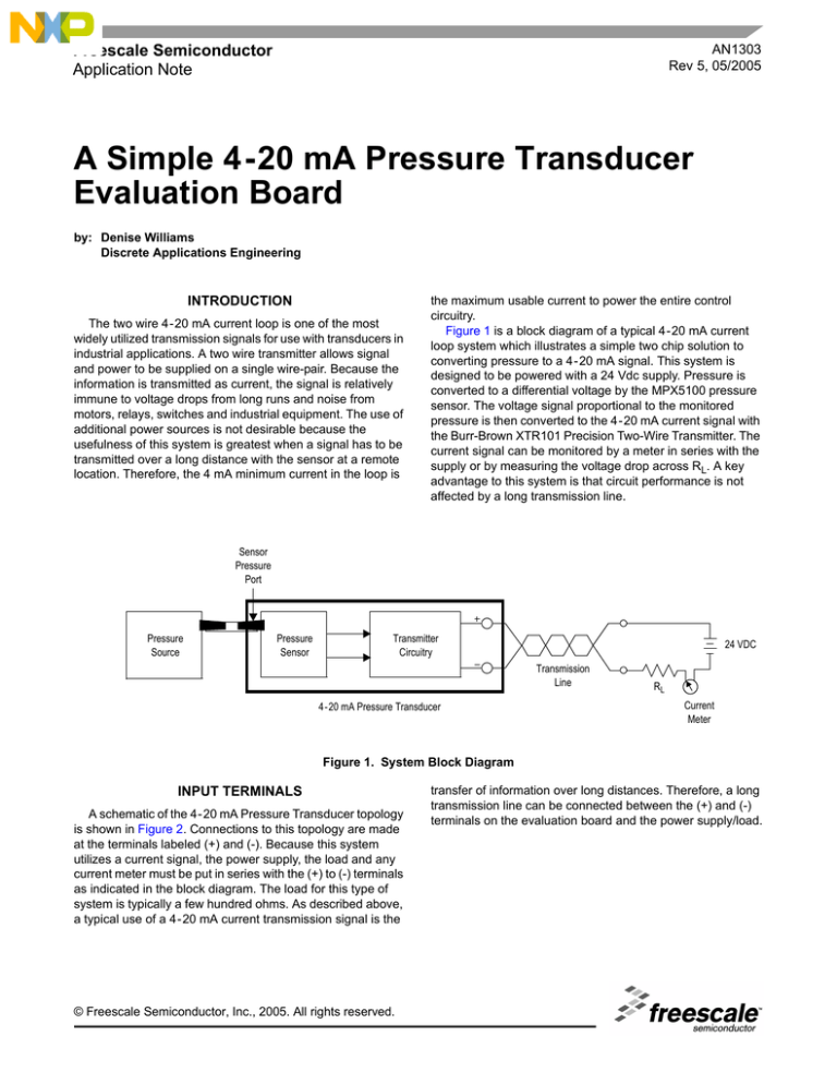
Figure 1 is a block diagram of a typical 4-20 mA current
loop system which illustrates a simple two chip solution to
converting pressure to a 4-20 mA signal. This system is
designed to be powered with a 24 Vdc supply. Pressure is
converted to a differential voltage by the MPX5100 pressure
sensor. The voltage signal proportional to the monitored
pressure is then converted to the 4-20 mA current signal with
the Burr-Brown XTR101 Precision Two-Wire Transmitter. The
current signal can be monitored by a meter in series with the
supply or by measuring the voltage drop across RL. A key
advantage to this system is that circuit performance is not
affected by a long transmission line.
Sensor
Pressure
Port
Pressure
Source
Pressure
Sensor
Transmitter
Circuitry
24 VDC
Transmission
Line
4-20 mA Pressure Transducer
RL
Current
Meter
Figure 1. System Block Diagram
INPUT TERMINALS
A schematic of the 4-20 mA Pressure Transducer topology
is shown in Figure 2. Connections to this topology are made
at the terminals labeled (+) and (-). Because this system
utilizes a current signal, the power supply, the load and any
current meter must be put in series with the (+) to (-) terminals
as indicated in the block diagram. The load for this type of
system is typically a few hundred ohms. As described above,
a typical use of a 4-20 mA current transmission signal is the
© Freescale Semiconductor, Inc., 2005. All rights reserved.
transfer of information over long distances. Therefore, a long
transmission line can be connected between the (+) and (-)
terminals on the evaluation board and the power supply/load.
2 mA
3
2
10 11
XDCR1
MPX7100
D2
1N4565A
6.4 V @ 0.5mA
4
R3
39
1
R5
50
R2
1K
4
5
12
U1
XTR101
6
3
1 2 14 7 13
R6
100K
+ 4-20 mA OUTPUT
R1
750
1/2 W
8
D1
1N4002
Q1
MPSA06
C1
0.01µF
9
- RETURN
R4
1M
4-20 mA Pressure Transducer
Figure 2. Schematic Diagram
PRESSURE INPUT
The device supplied on this topology is an MPX5100DP,
which provides two ports. P1, the positive pressure port, is on
top of the sensor and P2, the vacuum port, is on the bottom of
the sensor. The system can be supplied up to 15 PSI of
positive pressure to P1 or up to 15 PSI of vacuum to P2 or a
differential pressure up to 15 PSI between P1 and P2. Any of
these pressure applications will create the same results at the
sensor output.
Circuit Description
The XTR101 current transmitter provides two one-milliamp
current sources for sensor excitation when its bias voltage is
between 12 V and 40 V. The MPX5100 series sensors are
constant voltage devices, so a zener, D2, is placed in parallel
with the sensor input terminals. Because the MPX5100 series
parts have a high impedance the zener and sensor
combination can be biased with just the two milliamps
available from the XTR101.
The offset adjustment is composed of R4 and R6. They are
used to remove the offset voltage at the differential inputs to
the XTR101. R6 is set so a zero input pressure will result in
the desired output of 4 mA.
R3 and R5 are used to provide the full scale current span of
16 mA. R5 is set such that a 15 PSI input pressure results in
the desired output of 20 mA. Thus the current signal will span
16 mA from the zero pressure output of 4 mA to the full scale
output of 20 mA. To calculate the resistor required to set the
full scale output span, the input voltage span must be defined.
The full scale output span of the sensor is 24.8 mV and is ∆VIN
to the XTR101. Burr-Brown specifies the following equation
for Rspan. The 40 and 16 mΩ values are parameters of the
XTR101.
Rspan
=
=
40 / [(16 mA / ∆Vin) - 0.016 mhos]
64 Ω
The XTR101 requires that the differential input voltage at
pins 3 and 4, V2 - V1 be less than 1V and that V2 (pin 4)
always be greater than V1 (pin 3). Furthermore, this
differential voltage is required to have a common mode of 4-6
volts above the reference (pin 7). The sensor produces the
differential output with a common mode of approximately 3.1
volts above its reference pin 1. Because the current of both 1
mA sources will go through R2, a total common mode voltage
of about 5.1 volts (1 kΩ x 2 mA + 3.1 volts = 5.1 volts) is
provided.
CONCLUSION
This circuit is an example of how the MPX5000 series
sensors can be utilized in an industrial application. It provides
a simple design alternative where remote pressure sensing is
required.
AN1303
2
Sensors
Freescale Semiconductor
Table 1. Parts List for 4-20 mA Pressure Transducer Evaluation Board
Designator
Quantity
Description
1
1
4
4
2
2
PC Board
Input/Output Terminals
1/2″ standoffs, Nylon threaded
1/2″ screws, Nylon
5/8″ screws, Nylon
4-40 nuts, Nylon
1
Capacitor
0.01 µF
D1
D2
1
1
Diodes
100 V Diode
6.4 V Zener
Q1
1
Transistor
NPN Bipolar
R1
R2
R3
R4
1
1
1
1
Resistors, Fixed
750 Ω
1 kΩ
39 Ω
1 MΩ
R5
R6
1
1
U1
XDCR1
C1
Rating
Manufacturer
Freescale
PHX CONT
Part Number
DEVB126
#1727010
50 V
1A
1N4002
1N4565A
Freescale
MPSA06
Resistors, Variable
50 Ω, one turn
100 KΩ, one turn
Bourns
Bourns
#3386P-1-500
#3386P-1-104
1
Integrated Circuit
Two wire current transmitter
Burr-Brown
XTR101
1
Sensor
High Impedance
Freescale
MPX5100DP
1/2 W
15 PSI
NOTE: All resistors are 1/4 W with a tolerance of 5% unless otherwise noted. All capacitors are 100 volt, ceramic capacitors with a tolerance
of 10% unless otherwise noted.
AN1303
Sensors
Freescale Semiconductor
3
How to Reach Us:
Home Page:
www.freescale.com
E-mail:
support@freescale.com
USA/Europe or Locations Not Listed:
Freescale Semiconductor
Technical Information Center, CH370
1300 N. Alma School Road
Chandler, Arizona 85224
+1-800-521-6274 or +1-480-768-2130
support@freescale.com
Europe, Middle East, and Africa:
Freescale Halbleiter Deutschland GmbH
Technical Information Center
Schatzbogen 7
81829 Muenchen, Germany
+44 1296 380 456 (English)
+46 8 52200080 (English)
+49 89 92103 559 (German)
+33 1 69 35 48 48 (French)
support@freescale.com
Japan:
Freescale Semiconductor Japan Ltd.
Headquarters
ARCO Tower 15F
1-8-1, Shimo-Meguro, Meguro-ku,
Tokyo 153-0064
Japan
0120 191014 or +81 3 5437 9125
support.japan@freescale.com
Asia/Pacific:
Freescale Semiconductor Hong Kong Ltd.
Technical Information Center
2 Dai King Street
Tai Po Industrial Estate
Tai Po, N.T., Hong Kong
+800 2666 8080
support.asia@freescale.com
For Literature Requests Only:
Freescale Semiconductor Literature Distribution Center
P.O. Box 5405
Denver, Colorado 80217
1-800-441-2447 or 303-675-2140
Fax: 303-675-2150
LDCForFreescaleSemiconductor@hibbertgroup.com
AN1303
Rev 5
05/2005
Information in this document is provided solely to enable system and software
implementers to use Freescale Semiconductor products. There are no express or
implied copyright licenses granted hereunder to design or fabricate any integrated
circuits or integrated circuits based on the information in this document.
Freescale Semiconductor reserves the right to make changes without further notice to
any products herein. Freescale Semiconductor makes no warranty, representation or
guarantee regarding the suitability of its products for any particular purpose, nor does
Freescale Semiconductor assume any liability arising out of the application or use of any
product or circuit, and specifically disclaims any and all liability, including without
limitation consequential or incidental damages. “Typical” parameters that may be
provided in Freescale Semiconductor data sheets and/or specifications can and do vary
in different applications and actual performance may vary over time. All operating
parameters, including “Typicals”, must be validated for each customer application by
customer’s technical experts. Freescale Semiconductor does not convey any license
under its patent rights nor the rights of others. Freescale Semiconductor products are
not designed, intended, or authorized for use as components in systems intended for
surgical implant into the body, or other applications intended to support or sustain life,
or for any other application in which the failure of the Freescale Semiconductor product
could create a situation where personal injury or death may occur. Should Buyer
purchase or use Freescale Semiconductor products for any such unintended or
unauthorized application, Buyer shall indemnify and hold Freescale Semiconductor and
its officers, employees, subsidiaries, affiliates, and distributors harmless against all
claims, costs, damages, and expenses, and reasonable attorney fees arising out of,
directly or indirectly, any claim of personal injury or death associated with such
unintended or unauthorized use, even if such claim alleges that Freescale
Semiconductor was negligent regarding the design or manufacture of the part.
Freescale™ and the Freescale logo are trademarks of Freescale Semiconductor, Inc.
All other product or service names are the property of their respective owners.
© Freescale Semiconductor, Inc. 2005. All rights reserved.
