APPLICATION NOTE
A Varactor Controlled Phase Shifter for PCS Base Station
Applications
Introduction
Power amplifiers in today’s base stations use compensation
techniques to reduce distortion. There are many well-known
compensation techniques available, all relying on similar
principles of phase and amplitude control. Therefore, most (and
possibly all) of the compensation techniques use the same control
components: voltage-controlled attenuators and voltagecontrolled phase shifters.
The quality of these control components strongly determines
compensation circuit performance. The ideal phase shifter
provides a linear (vs. voltage) 0 to 360 degrees phase shift with
0 dB change in the signal level; similarly, the ideal attenuator
would provide a linear (vs. voltage) attenuation change with a
0-degree phase shift between attenuation settings.
This Application Note describes the design of a high-performance
phase shifter for PCS-band base station applications. The phase
shifter uses Skyworks low-cost SMV1245-011 varactor as the
phase-control element and the HY19-12, 90-degree hybrid. The
PCS band was selected because the large number of PCS
infrastructure base stations requires an efficient, low-cost
solution. However, the methodology of this design is applicable to
other wireless platforms.
Phase Shifter Fundamentals
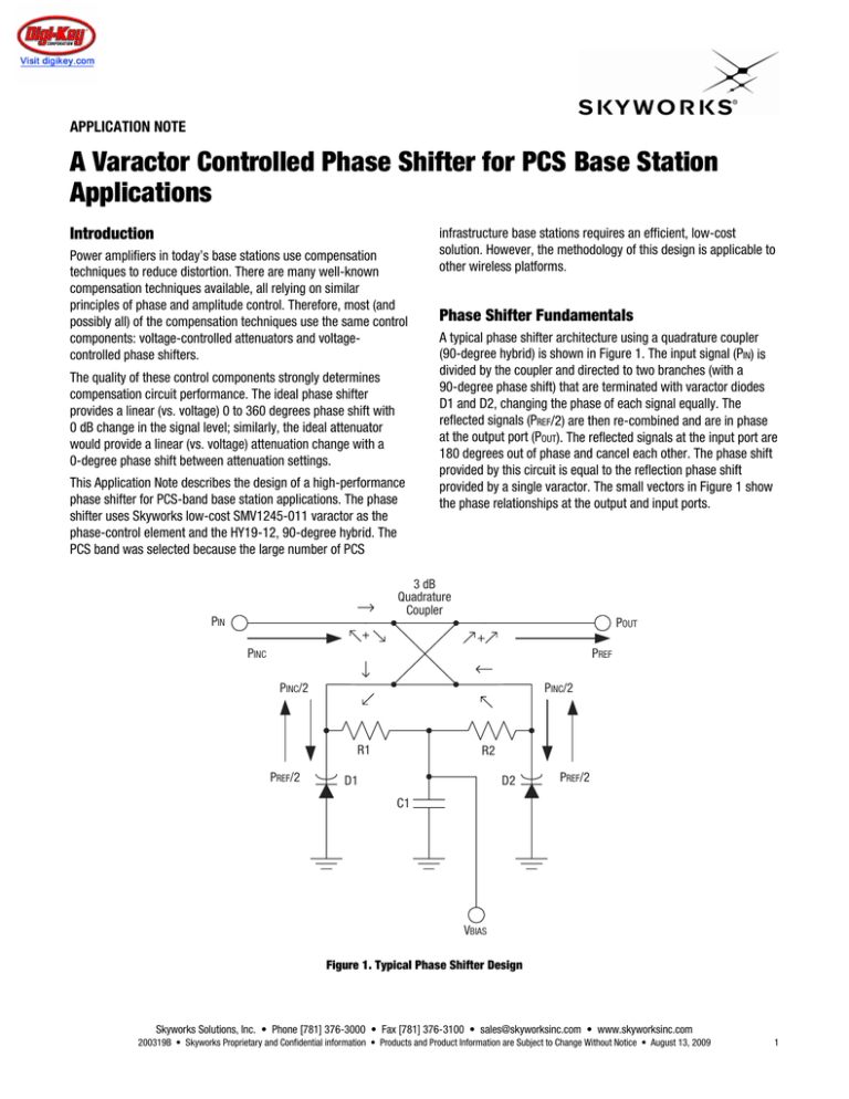
A typical phase shifter architecture using a quadrature coupler
(90-degree hybrid) is shown in Figure 1. The input signal (PIN) is
divided by the coupler and directed to two branches (with a
90-degree phase shift) that are terminated with varactor diodes
D1 and D2, changing the phase of each signal equally. The
reflected signals (PREF/2) are then re-combined and are in phase
at the output port (POUT). The reflected signals at the input port are
180 degrees out of phase and cancel each other. The phase shift
provided by this circuit is equal to the reflection phase shift
provided by a single varactor. The small vectors in Figure 1 show
the phase relationships at the output and input ports.
3 dB
Quadrature
Coupler
PIN
POUT
PINC
PREF
PINC/2
PINC/2
R1
PREF/2
R2
D2
D1
PREF/2
C1
VBIAS
Figure 1. Typical Phase Shifter Design
Skyworks Solutions, Inc. • Phone [781] 376-3000 • Fax [781] 376-3100 • sales@skyworksinc.com • www.skyworksinc.com
200319B • Skyworks Proprietary and Confidential information • Products and Product Information are Subject to Change Without Notice • August 13, 2009
1
APPLICATION NOTE • VARACTOR CONTROLLED PHASE SHIFTER FOR PCS BASE STATIONS
degrees. If both were connected in series, the ideal result would
be a 360-degree phase shift change.
A circulator terminated by a varactor may also be used to
separate the reflected and incident waves and provide a phase
shift. However, this solution would be costly. Instead, the circuit in
Figure 1 provides a lower cost alternative, although it uses two
phase shifting varactor circuits.
Figure 3 shows that adding a fixed inductor to a variable capacitor
increases the phase shift range. In this case, 6 nH was added at
1.95 GHz, resulting in a phase shift of approximately 280 degrees.
However, a continued increase of inductance reduces the effect of
the varactor capacitance range and leads to a degradation of the
overall phase shift range. Installing an additional capacitor (CPAR)
in parallel with the LC varactor network shown in Figure 4,
reduces this effect.
The varactor components in Figure 1 act as ideal, lossless
reactive loads with a reflection coefficient from 0 degrees (open
circuit – zero varactor capacitance) to –180 degrees (short circuit
– infinite varactor capacitance). The reflection phase shift for
different elementary circuits was calculated and is shown in
Figure 2. For an ideal variable capacitor that changes from 0 pF to
infinity, a total phase shift from 0 to –180 degrees occurs. For an
ideal variable inductor, the phase changes from –180 to 0
0
Reflection Phase Shift (Deg)
S11
S11
–60
–120
Capacitance (pF)
–180
–240
–300
Inductance (nH)
–360
0
2
4
6
8
10
12
14
16
18
20
Inductance (nH), Capacitance (pF)
Figure 2. Reflection (S11) Phase Shift for Elementary L and C Circuits
(Frequency = 1.95 GHz)
Reflection Phase Shift (Deg)
0
S11
–60
–120
Series Resonance
–180
–240
–300
–360
0
1
2
3
4
5
Capacitance (pF)
Figure 3. Reflection (S11) Phase Shift for Series LC Circuit
(Frequency = 1.95 GHz, Inductance = 6 nH)
Skyworks Solutions, Inc. • Phone [781] 376-3000 • Fax [781] 376-3100 • sales@skyworksinc.com • www.skyworksinc.com
2
August 13, 2009 • Skyworks Proprietary and Confidential information • Products and Product Information are Subject to Change Without Notice • 200319B
APPLICATION NOTE • VARACTOR CONTROLLED PHASE SHIFTER FOR PCS BASE STATIONS
LSER
S11
RS
RBIAS
CPAR
VCTL
RF Ground
CVAR
Figure 4. Equivalent Circuit of the Practical Phase Shifting Element
0
RS = 1 Ω,
RBIAS = 100 k
–0.1
S11 (dB)
–0.2
–0.3
RS = 1 Ω,
RBIAS = 3 k
–0.4
–0.5
–0.6
–0.7
–0.8
–270
RS = 0 Ω, RBIAS = 1 k
–240
–210
–180
–150
–120
–90
–60
S11 (Deg)
Figure 5. S11 State Chart for CVAR = 0 to 10 pF
The components shown in Figure 4 are used in a typical design.
Two additional resistive components are included: the parasitic
varactor series resistance (RS) and the added bias resistor (RBIAS).
Figure 5 shows the calculated loss, S11, for different
combinations of RS and RBIAS.
The varactor RS introduces most loss at maximum capacitance
(highest current in the varactor path). However, the bias
resistance, in parallel with the varactor, introduces the highest
loss at low capacitance, below the 180-degree phase shift point,
where resonance occurs. From linear circuit theory, this
resonance also depends on the value of RBIAS. When these loss
factors are taken into account, some flattening of the amplitude
response may result, as shown in Figure 5.
In reality, the varactor resistance, RS, may be a function of bias
(reverse) voltage. In some “very” hyperabrupt junction varactors,
the series resistance may vary 2 to 5 times from its maximum at
0 V to a minimum at the punch-through voltage. However, the
series resistance of the SMV1245-011 used in this design is
constant for the range of applied voltage.
The Phase Shifter Circuit Model
The circuit model (used for the Libra IV CAD software application)
is shown in Figure 6. A quadrature hybrid (HYB1) is used with 0.6
dB loss, which effectively simulates the HY19-12 used in our
design. Capacitors C1 and C2 are internal components within the
HY19-12 that isolate the DC paths from input and output ports.
The 0.5 dB loss pad (PAD1) simulates the total loss of the
input/output interface in the circuit board. In reality, the effect of
the input/output interface, including SMA transitions and
microstrip lines, is more complex than the pad used in the model.
The simplification is appropriate because the model concentrates
on the phase and amplitude response vs. control voltage, which is
not affected by the performance of the input/output interface.
Skyworks Solutions, Inc. • Phone [781] 376-3000 • Fax [781] 376-3100 • sales@skyworksinc.com • www.skyworksinc.com
200319B • Skyworks Proprietary and Confidential information • Products and Product Information are Subject to Change Without Notice • August 13, 2009
3
APPLICATION NOTE • VARACTOR CONTROLLED PHASE SHIFTER FOR PCS BASE STATIONS
PIPAD
PAD1
Z1 = 50
Z2 = 50
DB = 0.40
HYB90
HYB1
C=3
L = 0.60
Port P2
Port P1
C1
1000 pF
C2
1000 pF
SRL1
R = RISER
L = LSER
L1
0.9 nH
SRLC1
R = 0.2 Ω
L = 1 nH
C = CPAR
DATA:
MSUB_Coupler
ER = 4.2
H = 0.32
T = 0.02
RHO = 0.75
RGH = 0
COND1 = Condition
COND2 = Condition 2
DIEL1 = Diel
DIEL2 = Diel2
HOLE = Hole
RES = Resi
L2
0.9 nH
smv1245
X1
C3
0.14 pF
SRL2
R = RISER
L = Lser
R2
RBIAS
DCVS
SRC1
DC = VCTL
R1
RBIAS
SRLC2
R = 0.2 Ω
L = 1 nH
C = CPAR
VAR_VAR:
VCTL = 1
LSER = 2.8 nH
CPAR = 1.5 pF
RISER = 0.6 Ω
RBIAS = 200 Ω
smv1245
X2
C4
0.14 pF
S1605
Figure 6. Phase Shifter Circuit Model
Inductors L1 and L2 (both 0.9 nH) effectively simulate the HY1912 lead and package inductances. Parallel capacitors SRLC1 and
SRLC2 are simulated as a series R-L-C network with a package
inductance of 0.75 nH and series resistance of 0.2 Ω. The
discrete inductors SRL1 and SRL2 are modeled as lossy parallel
R-L-C networks with series resistance, RlSER = 0.6 Ω, and parallel
capacitance equal to 0.14 pF, which is typical for the majority of
multilayer inductors with inductance values within 2 to 5 nH.
CV =
C JO
⎛ VR
⎜⎜ 1 +
⎝ VJ
⎞
⎟⎟
⎠
M
+ CP
Where: CV = Total varactor capacitance (pF)
CJO = Zero-bias junction capacitance (pF)
VR = Reverse DC voltage (V)
VJ
= Junction potential (V)
SMV1245-011 SPICE Model
M
= Grading coefficient
The SMV1245-011 is a low capacitance, hyperabrupt varactor
diode in an SOD-323 package.
CP = Parasitic package capacitance (pF)
The SPICE model for the SMV1245-011 varactor diode, defined
for the Libra IV environment, is shown in Figure 7 with a
description of the parameters used.
Table 1 describes the model parameters and provides default
values appropriate for silicon varactor diodes that may be used by
the Libra IV (or similar) simulator.
According to the SPICE model, the varactor capacitance, CV, is a
function of the applied reverse DC voltage, VR, and may be
expressed as follows:
The above equation is a mathematical expression of the
capacitance characteristic. The model is most accurate for abrupt
junction varactors such as Skyworks SMV1408-001. However, for
hyperabrupt junction varactors, the model is less accurate
because the coefficients are dependent on the applied voltage.
To improve the equation for hyperabrupt junction varactors, the
coefficients need to be optimized for the best capacitance vs.
voltage fit. Such simulated coefficients may not have physical
meaning.
Skyworks Solutions, Inc. • Phone [781] 376-3000 • Fax [781] 376-3100 • sales@skyworksinc.com • www.skyworksinc.com
4
August 13, 2009 • Skyworks Proprietary and Confidential information • Products and Product Information are Subject to Change Without Notice • 200319B
APPLICATION NOTE • VARACTOR CONTROLLED PHASE SHIFTER FOR PCS BASE STATIONS
CP
0.47 pF
SRL
Series_R_L
R=2Ω
L = 2 nH
Port Anode
Port = 2
Port Cathode
Port = 1
DIODE
Diod1
Area = 1
Model = SMV1245
Mode = Nonlinear
DIODEM
SMV_1245
IS = 1.00E–14
RS = 0
N=1
TT = 0
CJO = 6.9E–12
VJ = 3.50
M = 1.70
EG = 1.11
XTI = 3
KF = 0
AF = 1
FC = 0.5
BV = 0
IBV = 1.00E–3
ISR = 0
NR = 2
IKF = 0
NBV = 1
IBVL = 0
NBVL = 1
TBV1 = 0
TNOM = 27
FFE = 1
S1606
Figure 7. SMV1245-011 SPICE Model
Table 1. Silicon Diode Default Values in Libra IV
Parameter
Unit
Silicon Varactor
Diode Default
Values
Saturation current. With N, determines the DC characteristics of the diode.
A
10–14
RS
Series resistance
Ω
0
N
Emission coefficient. With IS, determines the DC characteristics of the diode.
–
1
TT
Transit time
sec
0
IS
Description
CJO
Zero-bias junction capacitance. With VJ and M, defines the nonlinear junction capacitance of the diode.
F
0
VJ
Junction potential. With VJ and M, defines the nonlinear junction capacitance of the diode.
V
1
M
Grading coefficient. With VJ and M, defines the nonlinear junction capacitance of the diode.
–
0.5
EG
Energy gap. With XTI, helps define the dependence of IS on temperature.
EV
1.11
XTI
Saturation current temperature exponent. With EG, helps define the dependence of IS on temperature.
–
3
KF
Flicker noise coefficient.
–
0
AF
Flicker noise exponent.
–
1
FC
Forward-bias depletion capacitance coefficient.
–
0.5
BV
Reverse breakdown voltage
V
Infinity
IBV
Current at reverse breakdown voltage
A
10-3
ISR
Recombination current parameter
A
0
NR
Emission coefficient for ISR
–
2
IKF
High injection knee current
A
Infinity
NBV
Reverse breakdown ideality factor
–
1
IBVL
Low-level reverse breakdown knee current
A
0
NBVL
Low-level reverse breakdown ideality factor
TBV1
Reverse breakdown voltage linear temperature coefficient
–
1
1/°C
0
TNOM
Nominal ambient temperature at which these model parameters were derived
°C
27
FFE
Flicker noise frequency exponent
–
1
Skyworks Solutions, Inc. • Phone [781] 376-3000 • Fax [781] 376-3100 • sales@skyworksinc.com • www.skyworksinc.com
200319B • Skyworks Proprietary and Confidential information • Products and Product Information are Subject to Change Without Notice • August 13, 2009
5
APPLICATION NOTE • VARACTOR CONTROLLED PHASE SHIFTER FOR PCS BASE STATIONS
Table 2. SPICE Parameters for the SMV1245-011 Varactor
CJO
(pF)
M
VJ
(V)
CP
(pF)
RS
(Ω)
LS
(nH)
6.9
1.7
3.5
0.47
2
2
PIN
M1
HY19-12
IN
POUT
ISO
D1, D2
SMV1245-011
0
L1
2.2 nH
C1
1.5 pF
90°
R1
200 Ω
R2
200 Ω
D1
L2
2.2 nH
D2
C2
100 pF
C3
1.5 pF
VCTL
Figure 8. Phase Shifter Circuit Diagram
SPICE model values for the capacitance, CV, of the SMV1245-011
used in the phase-shifter design are provided in Table 2. Note
that, in the Libra model, CP is given in picofarads, while CGO is
provided in farads to comply with the default unit system used in
Libra.
Phase Shifter Design, Materials, and Layout
The circuit diagram for the phase shifter is shown in Figure 8 and
the PC board layout is shown in Figure 9. A Bill of Materials for
the phase shifter is provided in Table 3.
The PC board is made of 0.5 mm thick, standard FR4 material
with two-sided copper (0.02 mm thick) metallization. For test
purposes, the RF signals were fed through SMA connectors.
The 90-degree hybrid coupler is Skyworks model HY19-12, a
GaAs I/C optimized for PCS band applications. Although it is
manufactured using GaAs, this product is passive and does not
require an external bias. All RF leads of the HY19-12 are DC
isolated, minimizing the number of added DC blocking capacitors.
Sufficient grounding is provided through the four vias under the
I/C body.
Performance Discussion
Measured performance with simulated data is shown in
Figures 10 and 11. Three sets of circuit values were measured
and analyzed as shown on the graphs. The largest phase shift,
240 degrees, occurred at LSER = 2.2 nH and CPAR = 2.0 pF for a
varactor voltage change from 0 to 12 V. In this case, the
amplitude variation was about ±1.5 dB.
For CPAR = 1.5 pF, there was an approximate 190 degree phase
shift with ±0.75 dB amplitude variation. With LSER = 2.2 nH and
CPAR = 1.8 pF, there was an approximate 220 degree phase shift
with ±1.2 dB amplitude variation.
It is interesting to note that the “linear” range of phase shift
(linear vs. voltage) is similar for the three designs and is about
120 degrees (from 60 to 180 degrees). The highest phase/voltage
sensitivity was for CPAR = 2.0 pF estimated at about 40 to 50 V.
Higher phase shift values are achievable with higher CPAR values,
but larger amplitude variations would occur.
The measured and simulated phase responses were noticeably
similar, validating the assumptions in the model that predict
phase properties. The simulated amplitude responses were not as
close to the measured data. Some of the discrepancies may be
attributed to the simplified, idealized model of the 90-degree
hybrid coupler.
Skyworks Solutions, Inc. • Phone [781] 376-3000 • Fax [781] 376-3100 • sales@skyworksinc.com • www.skyworksinc.com
6
August 13, 2009 • Skyworks Proprietary and Confidential information • Products and Product Information are Subject to Change Without Notice • 200319B
APPLICATION NOTE • VARACTOR CONTROLLED PHASE SHIFTER FOR PCS BASE STATIONS
Figure 9. Phase Shifter PCB Layout
Table 3. Phase Shifter Bill of Materials
Component
Value
Size
Manufacturer
Part Number
C1, C3
1 pF
0603
AVX/Kyocera
CM105CG1ROK10AB
C2
100 pF
0603
AVX/Kyocera
CM105CG200K10AB
M1
–
SOIC-8
Skyworks Solutions
HY19-12
R1, R2
200 Ω
0603
AVX
CR105-201J-T
D1, D2
–
SOD-323
Skyworks Solutions
SMV1245-011
L1, L2
2.2 nH
0603
ACX
HI1608-1B2N2_N_K_B
In this design, only the SMV1245-011 varactor diode was
considered out of a large selection of available varactors.
Varactors with higher tuning sensitivity, such as the SMV1247 or
SMV1263, provide a higher range of phase shift but with more
amplitude variation. Abrupt junction varactors from the SMV1400
series operate with lower tuning sensitivities and less phase
control but with lower loss and better amplitude linearity.
For additional information, refer to the Skyworks Application Note,
Varactor SPICE Models for RF VCO Applications, document
number 200315.
Skyworks Solutions, Inc. • Phone [781] 376-3000 • Fax [781] 376-3100 • sales@skyworksinc.com • www.skyworksinc.com
200319B • Skyworks Proprietary and Confidential information • Products and Product Information are Subject to Change Without Notice • August 13, 2009
7
APPLICATION NOTE • VARACTOR CONTROLLED PHASE SHIFTER FOR PCS BASE STATIONS
240
LSER = 2.2 nH,
CPAR = 2.0 pF (simul)
S21 (Deg)
180
LSER = 2.2 nH,
CPAR = 1.8 pF (simul)
120
60
LSER = 2.2 nH,
CPAR = 1.5 pF (simul)
0
0
1
2
3
4
5
6
7
8
9 10 11 12
Control Voltage (V)
Figure 10. Measured and Simulated Phase Response
–2.0
LSER = 2.2 nH,
CPAR = 1.5 pF (simul)
–2.5
–3.0
LSER = 2.2 nH,
CPAR = 2.0 pF (simul)
S21 (dB)
–3.5
–4.0
–4.5
–5.0
LSER = 3.3 nH,
CPAR = 1.5 pF (simul)
–5.5
–6.0
–6.5
0
1
2
3
4
5
6
7
8
9 10 11 12
Control Voltage (V)
Figure 11. Measured and Simulated Amplitude Response
Skyworks Solutions, Inc. • Phone [781] 376-3000 • Fax [781] 376-3100 • sales@skyworksinc.com • www.skyworksinc.com
8
August 13, 2009 • Skyworks Proprietary and Confidential information • Products and Product Information are Subject to Change Without Notice • 200319B
APPLICATION NOTE • VARACTOR CONTROLLED PHASE SHIFTER FOR PCS BASE STATIONS
Copyright © 2002, 2003, 2004, 2005, 2009 Skyworks Solutions, Inc. All Rights Reserved.
Information in this document is provided in connection with Skyworks Solutions, Inc. (“Skyworks”) products or services. These materials, including the information contained herein, are provided by
Skyworks as a service to its customers and may be used for informational purposes only by the customer. Skyworks assumes no responsibility for errors or omissions in these materials or the
information contained herein. Skyworks may change its documentation, products, services, specifications or product descriptions at any time, without notice. Skyworks makes no commitment to
update the materials or information and shall have no responsibility whatsoever for conflicts, incompatibilities, or other difficulties arising from any future changes.
No license, whether express, implied, by estoppel or otherwise, is granted to any intellectual property rights by this document. Skyworks assumes no liability for any materials, products or
information provided hereunder, including the sale, distribution, reproduction or use of Skyworks products, information or materials, except as may be provided in Skyworks Terms and Conditions
of Sale.
THE MATERIALS, PRODUCTS AND INFORMATION ARE PROVIDED “AS IS” WITHOUT WARRANTY OF ANY KIND, WHETHER EXPRESS, IMPLIED, STATUTORY, OR OTHERWISE, INCLUDING FITNESS FOR A
PARTICULAR PURPOSE OR USE, MERCHANTABILITY, PERFORMANCE, QUALITY OR NON-INFRINGEMENT OF ANY INTELLECTUAL PROPERTY RIGHT; ALL SUCH WARRANTIES ARE HEREBY EXPRESSLY
DISCLAIMED. SKYWORKS DOES NOT WARRANT THE ACCURACY OR COMPLETENESS OF THE INFORMATION, TEXT, GRAPHICS OR OTHER ITEMS CONTAINED WITHIN THESE MATERIALS. SKYWORKS
SHALL NOT BE LIABLE FOR ANY DAMAGES, INCLUDING BUT NOT LIMITED TO ANY SPECIAL, INDIRECT, INCIDENTAL, STATUTORY, OR CONSEQUENTIAL DAMAGES, INCLUDING WITHOUT LIMITATION,
LOST REVENUES OR LOST PROFITS THAT MAY RESULT FROM THE USE OF THE MATERIALS OR INFORMATION, WHETHER OR NOT THE RECIPIENT OF MATERIALS HAS BEEN ADVISED OF THE
POSSIBILITY OF SUCH DAMAGE.
Skyworks products are not intended for use in medical, lifesaving or life-sustaining applications, or other equipment in which the failure of the Skyworks products could lead to personal injury,
death, physical or environmental damage. Skyworks customers using or selling Skyworks products for use in such applications do so at their own risk and agree to fully indemnify Skyworks for any
damages resulting from such improper use or sale.
Customers are responsible for their products and applications using Skyworks products, which may deviate from published specifications as a result of design defects, errors, or operation of
products outside of published parameters or design specifications. Customers should include design and operating safeguards to minimize these and other risks. Skyworks assumes no liability for
applications assistance, customer product design, or damage to any equipment resulting from the use of Skyworks products outside of stated published specifications or parameters.
Skyworks, the Skyworks symbol, and “Breakthrough Simplicity” are trademarks or registered trademarks of Skyworks Solutions, Inc., in the United States and other countries. Third-party brands
and names are for identification purposes only, and are the property of their respective owners. Additional information, including relevant terms and conditions, posted at www.skyworksinc.com,
are incorporated by reference.
Skyworks Solutions, Inc. • Phone [781] 376-3000 • Fax [781] 376-3100 • sales@skyworksinc.com • www.skyworksinc.com
200319B • Skyworks Proprietary and Confidential information • Products and Product Information are Subject to Change Without Notice • August 13, 2009
9
