Synchronous Serial IO
TRISC6
TRISC[6]
Must be “0” so that RC6/TX/CK pin is an output.
TRISC7
TRISC[7]
Must be “1” so that RC7/RX/DT pin is an input.
331
11.4 THE SERIAL PERIPHERAL INTERFACE (SPI)
The Serial Peripheral Interface, originally developed by Motorola, is a three-wire synchronous serial link that has developed into a de facto standard due to its adoption by
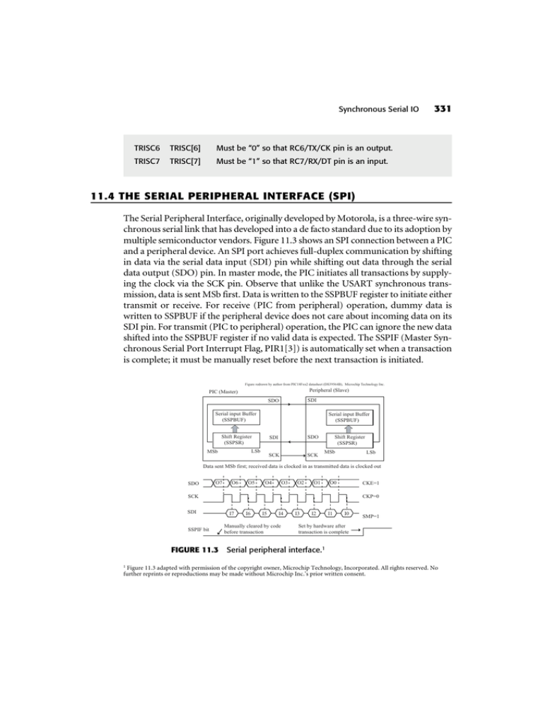
multiple semiconductor vendors. Figure 11.3 shows an SPI connection between a PIC
and a peripheral device. An SPI port achieves full-duplex communication by shifting
in data via the serial data input (SDI) pin while shifting out data through the serial
data output (SDO) pin. In master mode, the PIC initiates all transactions by supplying the clock via the SCK pin. Observe that unlike the USART synchronous transmission, data is sent MSb first. Data is written to the SSPBUF register to initiate either
transmit or receive. For receive (PIC from peripheral) operation, dummy data is
written to SSPBUF if the peripheral device does not care about incoming data on its
SDI pin. For transmit (PIC to peripheral) operation, the PIC can ignore the new data
shifted into the SSPBUF register if no valid data is expected. The SSPIF (Master Synchronous Serial Port Interrupt Flag, PIR1[3]) is automatically set when a transaction
is complete; it must be manually reset before the next transaction is initiated.
Figure redrawn by author from PIC18Fxx2 datasheet (DS39564B), Microchip Technology Inc.
Peripheral (Slave)
PIC (Master)
SDI
SDO
Serial input Buffer
(SSPBUF)
Serial input Buffer
(SSPBUF)
Shift Register
(SSPSR)
LSb
MSb
SDI
SDO
SCK
SCK
Shift Register
(SSPSR)
MSb
LSb
Data sent MSb first; received data is clocked in as transmitted data is clocked out
SDO
O7
O6
O5
O4
O3
O2
O1
O0
CKE=1
CKP=0
SCK
SDI
SSPIF bit
I7
I6
I5
I4
Manually cleared by code
before transaction
I3
I2
I1
I0
SMP=1
Set by hardware after
transaction is complete
FIGURE 11.3 Serial peripheral interface.1
1
Figure 11.3 adapted with permission of the copyright owner, Microchip Technology, Incorporated. All rights reserved. No
further reprints or reproductions may be made without Microchip Inc.’s prior written consent.
332
Microprocessors
Configuration bits CKE (clock edge select, SSPSTAT[6]), CKP (clock polarity
select, SSPCON1[4]), and SMP (input sample select, SSPSTAT[7]) provide considerable flexibility for data transmit and receive. The CKE and CKP bits are used
for transmit; CKE selects the active clock edge for SDO valid data while CKP selects
the clock polarity, either idle high or idle low. Figure 11.4 shows the four cases for
the CKE and CKP bit settings. Observe that for CKP = 0 (clock idle low), CKE =
0 has SDO stable on the falling clock edge, while CKE = 1 provides valid SD0 data
on the rising clock edge. For CKP = 1 (clock idle high) this is reversed, with CKE
= 0 providing stable SD0 data on the rising clock edge and CKE = 1 makes SDO
valid on the falling clock edge. The SMP bit determines where the SDI input is sampled during receive, either in the middle of the SCK period (SMP = 0) or at the
end of the SCK period (SMP = 1) as shown in Figure 11.4. The required settings
for the CKE, CKP, and SMP bits depend upon the target peripheral.
Figure redrawn by author from PIC18Fxx2 datasheet (DS39564B), Microchip Technology Inc.
Write to SSPBUF
SCK
(CKP = 0, CKE = 0)
SCK
(CKP = 1, CKE = 0)
SCK
(CKP = 0, CKE = 1)
SCK
(CKP = 1, CKE = 1)
SDO (CKE = 0)
b7
b6
b5
b4
b3
b2
b1
b0
SDO (CKE = 1)
b7
b6
b5
b4
b3
b2
b1
b0
SDI (SMP = 0)
b7
b6
b5
b4
b3
b2
b1
b0
Input Sample
(SMP = 0)
SDI (SMP = 1)
Input Sample
(SMP = 1)
SSPIF
SSPSR to SSPBUF
FIGURE 11.4
b7
b6
b5
b4
b3
b2
b1
b0
Next Q4 cycle
after Q2 ?
CKE/CKP/SMP cases for SPI transmission.2
The SCK frequency is controlled by the SSPM (Synchronous Serial Port Mode
select, SSPCON1[3:0]) bits. The four choices for master mode are “0011” (Timer2
output divided by 2), “0010” (FOSC/64), “0001” (FOSC/16), and “0000”
2
Figure 11.4 adapted with permission of the copyright owner, Microchip Technology, Incorporated. All rights reserved. No
further reprints or reproductions may be made without Microchip Inc.’s prior written consent.
Synchronous Serial IO
333
(FOSC/4). Table 11.3 summarizes the configuration bits used for SPI mode transfers. Observe that SCK, SDI, and SDO are shared with the PORTC pins and that
TRISC must be used to configure these pins as inputs or outputs as shown in Table 11.3.
TABLE 11.3 Control Registers/Bits for SPI Master Mode Configuration
Name
SFR(bit)
Comment
SSPEN
SSPCON1[5]
Must be “1” to enable SCK, SDO, SDI pins
SSPM[3:]
SSPCON1[3:0]
“0011”, SPI Master Mode, SCK= TMR2/2
“0010”, SPI Master Mode, SCK= FOSC/64
“0001”, SPI Master Mode, SCK = FOSC/16
“0000”, SPI Master Mode, SCK = FOSC/4
CKE
SSPSTAT[6]
For CKP = 0:
“1”: SDO valid on rising SCK edge
“0”: SDO valid on falling SCK edge
For CKP = 1:
“1”: SDO valid on falling SCK edge
“0”: SDO valid on rising SCK edge
CKP
SSPCON1[4]
“1”: SCK idle high, “0”: SCK idle low
SMP
SSPSTAT[7]
“1”: sample SDI at end of SCK in master mode
“0”: sample SDI in middle of SCK in master mode
(must be a “0” in slave mode)
SSPIF
PIR1[3]
Set to “1” after transmission complete
TRISC3
TRISC[3]
Must be “0” so that RC3/SCK/SCL pin is an output
TRISC4
TRISC[4]
Must be “1” so that RC4/SDI/SDA pin is an input
TRISC5
TRISC[5]
Must be “0” so that RC5/SDO pin is an output
334
Microprocessors
Sample Question: What are the required settings for CKP, CKE, and SMP for the SPI
waveform specification shown in Figure 11.5?
SDO
O7
O6
SDI
I7
I6
FIGURE 11.5
What are the needed CKE, CKP, and SPM
settings for this transfer?
~
~
SCK
~
~
~ ~
~ ~
Answer: The clock is idle high, so CKP = 1. Output data is stable on the rising clock edge, so CKE = 0 by Figure 11.4. Data is sampled in the middle of
SCK, so SMP = 0.
A sample SPI waveform specification.
11.5 SPI EXAMPLES: A DIGITAL POTENTIOMETER AND
A SERIAL EEPROM
Many peripheral devices such as analog-to-digital converters, digital-to-analog
converters, digital potentiometers, and serial EEPROMs are available with SPIcompatible interfaces. As discussed previously, the advantage of a serial interface is
low pin count at the cost of reduced IO bandwidth.
The MCP41xxx Digital Potentiometer
Figure 11.6 shows an application of a MCP41xxx digital potentiometer [12] as a
contrast control for the LCD module discussed in Chapter 8, “The PIC18Fxx2:
System Startup and Parallel Port IO.” A potentiometer is a device that provides a
variable resistance. An analog potentiometer typically has three terminals; between
two of the terminals the potentiometer’s full resistance is available (reference terminals PA0, PB0 in Figure 11.6). The third terminal is called the wiper (terminal
PW0 in Figure 11.6), and this terminal provides a variable resistance when measured between the wiper and either one of the reference terminals. When the two
reference terminals are connected to Vdd and ground, changing the wiper setting
varies the voltage on the wiper terminal between Vdd and ground. An analog potentiometer’s wiper setting is changed via some mechanical interface; for example,
turning a shaft. A digital potentiometer’s wiper setting is changed using a parallel
or serial interface, with serial interfaces being the most common.
Synchronous Serial IO
Vdd
335
MCP41xxx
LCD
Vdd
PA0
PIC
PW0
RB4
SDO
SCK
FIGURE 11.6
CS#
SI
SCK
PB0
Vss
Vdd
VL
Vss
PW0 voltage varies
between 0 and Vdd, used
for contrast control to LCD
PIC to MCP41xxx digital potentiometer interface.
The MCP41xxx digital potentiometer comes in 10 K (MCP41010), 50 K
(MCP41050), and 100 K (MCP41100) configurations and uses an SPI port for setting the 8-bit wiper register for the potentiometer. In the configuration shown in
Figure 11.6, a wiper value of 255 sets the PW0 output voltage to approximately
255/256 * Vdd, while a value of 0 sets the PW0 output voltage to ground. The
wiper register is set to 0x80 on power-up. Higher potentiometer values reduce the
static current that is drawn by the potentiometer when it is active. For example, a
50 K potentiometer with Vdd = 5 V draws 5 V/50 K = 100 µA static current
through the potentiometer resistance, while a 100 K potentiometer reduces this
current by 50% to 50 µA.
Figure 11.7 shows the command protocol for the MCP41xxx. Each transaction
consists of 2 bytes, a command byte and a data byte. The CS# (Chip Select) input
must be brought low to enable the device before any data is sent and brought high
after transmission is finished in order to execute the command. The wiper register
is set by the command byte 0x11 followed by the wiper register value. The shutdown command opens (disconnects) the potentiometer by opening the PA0 terminal and shorting the PW0 and PB terminals. This reduces total static current
draw of the MCP41xxx to less than 1 µA. The data byte for the shutdown command is ignored but it still must be sent for the command to be recognized. If
MCP41xxx shutdown mode were to be used with the LCD application of Figure
11.6, you would want to reverse the PA0 and PB0 connections so that VL of the
LCD is shorted to Vdd during shutdown, blanking the display. This would mean
that a wiper code of 255 sets the PW0 voltage to near ground, while a code of 0 sets
the PW0 voltage to Vdd.
336
Microprocessors
Input data latched
on rising edge
Must be low for
device enable
Potentiometer data registers
loaded on rising edge
CS#
1
2
3 4
5
6
7
8
9
2
10 11 12 13 14 15
SCK
MSb
SI
LSb MSb
LSb
X X C1 C0 X X X P0 D7 D6 D5 D4 D3 D2 D1 D0
Data Byte
Command Byte
X : don’t care bits
C1, C0: command bits, “01” set wiper register to data byte, “10” shutdown
P0: must be “1” to select potentiometer for command
Sample commands: 0x11 - write wiper register, 0x21 - shutdown potentiometer
FIGURE 11.7 MCP41xxx command protocol.
Figure 11.8 gives code for testing the PIC to MCP41xxx interface. The
while(1){} loop of main() prompts the user for an 8-bit value and sends this as the
wiper register value to the MCP41xxx via the spi_setpotmtr(unsigned char c){}
function. Within the spi_setpotmtr() function, the chip select of the MCP41xxx is
brought low by the command bitclr(PORTB, POTCS) statement, where POTCS is
defined as 4. This is equivalent to writing RB4 = 0, but the bitclr macro is used so
that changing to a different PORTB pin for chip select only requires modifying the
#define POTCS 4 statement. After the chip select is asserted, the command byte
(0x11) is written followed by the data byte passed to the function in the c parameter.
Observe that after a byte is written to SSPBUF, the while(!SSPIF) loop waits for the
SSPIF to become nonzero, indicating that the transmission is finished. The
statement SSPIF = 0 is then used to manually reset the SSPIF bit before the next
transmission. The MCP41xxx chip select is negated by the bitset(PORTB,POTCS)
statement before exiting spi_setpotmtr(). The SPI initialization code in main() uses
a positive clock polarity (CKP = 0) and data transmitted on the rising edge (CKE
= 1), as that matches the SPI specifications in the MCP41xxx datasheet. The SCK
frequency of FOSC/16 gives an SCK of approximately 1.8 MHz for the 29.4912
MHz FOSC of the PIC18F242 reference board. This SCK frequency is safely below
the maximum 10 MHz SCK frequency of the MCP41050 device used for testing.
Synchronous Serial IO
337
#include
<pic18.h>
#include "config.h"
Include files for configuration bits and
#include "serial.c"
asynchronous serial port IO
#include "serio.c"
}
//RB4 is select for potentiometer
#define POTCS 4
Function for setting potentiometer wiper register
spi_setpotmtr(unsigned char c){
bitclr(PORTB, POTCS); // select potmtr
SSPBUF = 0x11; // write command
while(!SSPIF); // wait until transmited
SSPIF = 0;
// reset
SSPBUF = c;
// write data
while(!SSPIF); // wait until transmited
SSPIF = 0;
// reset
bitset(PORTB, POTCS); // deselect potmtr
}
main(void){
unsigned char pv;
// set select line for output
bitclr(TRISB,POTCS);
bitset(PORTB, POTCS); // deselect pot
Assert Chip Select
Write command byte, wait for
transmit to end, then reset SSPIF
}
data byte, wait for
} Write
transmit to end, then reset SSPIF
Negate Chip Select
RB4 as an output, ensure
} Configure
that it is high, deselecting MCP41xxx
serial_init(95,1); // 19200 in HSPLL mode, crystal = 7.3728 MHz
// configure SPI port for potentiometer
CKE = 1; // data transmitted rising edge of SCK
CKP = 0; // clk idle is low
bitclr(TRISC,3); //SCK, output
bitclr(TRISC,5); // SDO, output
bitset(TRISC,4); // SDI pin is input, unused
// SPI Master Mode FOSC/16
SSPM3 = 0; SSPM2 = 0; SSPM1 = 0; SSPM0 = 1;
SSPEN = 0; // reset Sync Serial port
SSPEN = 1; // enable Sync Serial port
SSPIF = 0; // clear SPIF bit
}
Configure SPI port.
Must use CKE=1, CKP=0
as that is compatible with
datasheet specs for
MCP41xxx.
Use FOSC/16, sets SCK
as approx. 1.8 Mhz for
29.49 MHz FOSC
pcrlf(); printf("Potentiometer test started"); pcrlf();
while(1) {
printf("Input value (0-255): ");
Prompt user for 8-bit input value,
scanf("%d", &pv);
send to potentiometer and
pcrlf();
printf("Sending %d to pot.",pv);
use voltmeter to check
pcrlf();
potentiometer output value.
spi_setpotmtr(pv);
}
}
}
ON THE CD
FIGURE 11.8
Test code for PIC to MCP41xxx interface.
The 25LC640 Serial EEPROM
Figure 11.9 shows a PIC18 to 25LC640 serial EEPROM [13] interface. The 25LC640
is a 64 Kb serial EEPROM with an internal 8K x 8 organization and uses an SPI
port for communication. The HOLD# input allows a data transfer to be interrupted
mid-stream and the WP# input disables write operations to the device. These capabilities are not needed in this example, so these pins are tied high to disable them.


