PVOA201
Rev. C
PVOA201
Ultralow Power / Low Noise, Negative Rail Input, Rail-to-Rail Output
Fully Differential Operational Amplifier and ADC Driver
The PVOA201 is a low power, low noise, fully-differential op amp with a rail-to-rail output and an input commonmode range including the negative power supply rail. This amplifier is an ideal candidate for low power data
acquisition systems, handhelds, and other portable devices where low power dissipation is important.
The amplifier features an adjustable output common mode control for optimizing the common mode level, ideal
for driving analog-to-digital converters. The device allows easy translation from single-ended signals to differential
signals on the input or on the output. The PVOA201 is also ideal for level shifting ground referenced signals to
common mode levels within the output common mode range of the amplifier.
With a low input referred voltage noise of 3.5nV/√𝐻𝐻𝐻𝐻 and single supply operation from +2.5V to +3.6V, the
PVOA201 is well suited for a variety of low power / low noise data acquisition and signal processing applications.
General Features
Fully Differential
Bandwidth: 165MHz, G=1
Slew Rate: 58 V/µs
Input Voltage Noise: 3.5nV/√Hz
Rail-to-Rail Output
Negative Rail Input
Output Common Mode Control
Power Supply:
Single Supply: +2.5V to +3.6V
Dual Supply: +/-1.25V to +/-1.8V
Supply Current: 1.15mA
• Small PCB area and layout
Package: TSSOP-8 lead
• Temp range: -40 to +85°C
•
•
•
•
•
•
•
•
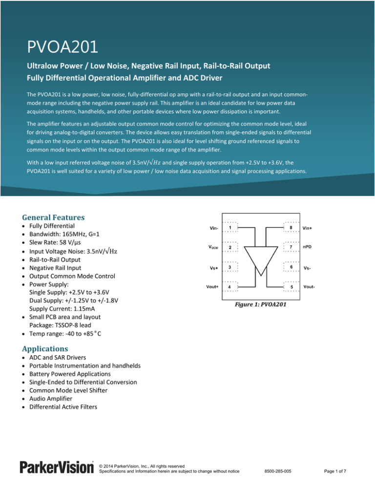
Figure 1: PVOA201
Applications
•
•
•
•
•
•
•
ADC and SAR Drivers
Portable Instrumentation and handhelds
Battery Powered Applications
Single-Ended to Differential Conversion
Common Mode Level Shifter
Audio Amplifier
Differential Active Filters
© 2014 ParkerVision, Inc., All rights reserved
Specifications and Information herein are subject to change without notice
8500-285-005
Page 1 of 7
PVOA201
Rev. C
Contents
General Features ________________________________________________________________________________ 1
Applications ____________________________________________________________________________________ 1
Figure 1: PVOA201 _____________________________________________________________________________________ 1
Pin Description _________________________________________________________________________________ 3
Figure 2: PVOA201 Pin Diagram ___________________________________________________________________________ 3
Absolute Minimum and Maximum Ratings ___________________________________________________________ 3
Electrical Specifications ___________________________________________________________________________ 4
Power Supply ___________________________________________________________________________________________
AC Performance _________________________________________________________________________________________
Input Characteristics ______________________________________________________________________________________
Output Characteristics ____________________________________________________________________________________
4
4
4
4
Applications Information _________________________________________________________________________ 6
Differential Input to Differential Output Amplifier ______________________________________________________________
Figure 3: Differential Input to Differential Output Amplifier ____________________________________________________
Single-Ended Input to Differential Output Amplifier _____________________________________________________________
Figure 4: Single-Ended Input to Differential Output Amplifier ___________________________________________________
Setting the Output Common Mode Voltage at Pin 2 VOCM. ________________________________________________________
Figure 5: Simplified VOCM Input ___________________________________________________________________________
6
6
6
6
6
6
Package Information _____________________________________________________________________________ 7
© 2014 ParkerVision, Inc., All rights reserved
Specifications and Information herein are subject to change without notice
8500-285-005
Page 2 of 7
PVOA201
Rev. C
Pin Description
Pin Number
1
2
3
4
5
6
7
8
Pin Name
VinVocm
Vs+
Vout+
VoutVsnPD
Vin+
Description
Inverting input
Common–mode control input
Positive power supply input
Non-inverting output
Inverting output
Negative power supply input
Amplifier power down input. Logic “low” places the device in sleep mode
Non-inverting input
8-Lead TSSOP Package, Top View
Figure 2: PVOA201 Pin Diagram
Absolute Minimum and Maximum Ratings
Parameter
PVOA201
Supply Voltage
Input / Output Voltage
Differential Input Voltage
ESD
Max Junction Temperature
Storage Temp
Symbol
Conditions
Min
Max
Unit
(VS- ) - 0.3
+3.6
(VS+ ) + 0.3
VS- to VS+
V
V
V
V
°C
°C
VS- to VS+
VIN+/- , VOUT+/- , VOCM
VID
Human Body (HBM)
TJ
TSTG
Operating
-40
© 2014 ParkerVision, Inc., All rights reserved
Specifications and Information herein are subject to change without notice
+125
+150
8500-285-005
Page 3 of 7
PVOA201
Rev. C
Electrical Specifications
TA = +25 ° C, VS+ - VS- = +3.3V, VOCM = (VS+ - VS- ) / 2, RF=RG=2K unless otherwise noted
Parameter
Symbol
Power Supply
Temperature Range
Power Supply
Supply Voltage
Supply Current
Conditions
Min
Typ
Max
-40
VDD3p3
IDD3p3
+PSRR
-PSRR
Power Supply Rejection
Power Down Current
Enable Voltage
nPD
2.5
PVOA201 “on”
PVOA201 “off”
2.25
3.3
1.15
Unit
125
°C
3.6
V
mA
dB
dB
µA
V
V
10
0.5
AC Performance
Small Signal Bandwidth
Large Signal Bandwidth
Differential Rising Slew Rate
Differential Falling Slew Rate
Settling Time to 0.1%
Harmonic Distortion
Input Characteristics
Input Voltage Noise
Input Current Noise
Input Bias Current
Input Bias Current Drift
Input Offset Voltage
Input Offset Voltage Drift
G=1
G=2
G=5
G=10
G=1, Vout=2Vp-p
2V Step
2V Step
Vout_diff=2Vp-p
160
98
40
19
9
58
58
43
MHz
MHz
MHz
MHz
MHz
V/µs
V/µs
ns
F=10kHz
F=10kHz
3.5
0.72
808
2.2
52
nV/√𝐻𝐻𝐻𝐻
pA/√𝐻𝐻𝐻𝐻
nA
nA/°C
µV
TMIN to TMAX
TMIN to TMAX
Differential
Common Mode
Input Resistance
Input Capacitance
Open-Loop Gain
RG=RF=4k
Common Mode Input Range
Common Mode Rejection Ratio
(Vs-)0.3
64
9
1
91
120
kΩ
MΩ
pF
dB
(Vs+)V
0.9
dB
Output Characteristics
Output Voltage Swing
Each single-ended output
Output Current Drive
© 2014 ParkerVision, Inc., All rights reserved
Specifications and Information herein are subject to change without notice
(Vs-) +0.15
to
(Vs+)-0.15
+/-14
mA
8500-285-005
Page 4 of 7
V
PVOA201
Parameter
Symbol
Conditions
Min
Typ
Max
Unit
+10
mV
Rev. C
VOCM Control
Gain
1
Common-mode Offset
-10
Input Bias Current
250
Input Impedance
50
(Vs-) +0.9
to
(Vs+)-0.8
VOCM Voltage Range
© 2014 ParkerVision, Inc., All rights reserved
Specifications and Information herein are subject to change without notice
8500-285-005
pA
kΩ
V
Page 5 of 7
PVOA201
Rev. C
Applications Information
Differential Input to Differential Output Amplifier
The PVOA201 is a fully differential operational amplifier
that can be configured in several different ways depending
on application. One of the most common uses for the
amplifier is to process differential input signals and
amplify these signals to differential outputs. In the
following diagram for simplicity, the VOCM and nPD pins are
not shown. The closed loop gain of the circuit is simply RF /
RG .
RF
Differential
Input
RG
VIN+
Differential
Output
VS+
+
_
VOUT-
PVOA201
VIN-
VOCM (pin 2) can be driven by connecting an external
voltage source to the pin. When externally driving the pin,
the guidelines detailed in the electrical specification
section should be followed as to not exceed the VOCM
range of (Vs-) +0.9Vdc to (Vs+)-0.8Vdc. For instance, using
a single supply voltage of +3.3V allows the user to adjust
the output common mode level between the limits +0.9V
to +2.5V. An external current is required to drive the VOCM
given by the following equation:
+
_
RG
Setting the Output Common Mode Voltage at Pin 2
VOCM.
The output common mode voltage of the operational
amplifier tracks the voltage at the VOCM pin. The VOCM pin
can be left unconnected. In this case, the output common
mode level of the amplifier will be held to mid-supply.
VOUT+
VS-
𝐼𝑉𝑂𝐶𝑀 =
2𝑉𝑂𝐶𝑀 − (𝑉𝑆+ − 𝑉𝑆− )
50𝑘Ω
A decoupling capacitor of at least 0.1uF is recommended
on the VOCM pin for noise reduction.
RF
Figure 3: Differential Input to Differential Output
Amplifier
Single-Ended Input to Differential Output Amplifier
Another application of the PVOA201 is to convert single
ended input signals to differential output signals. The
signals can be ground referenced as illustrated in Figure 4
below. Once again, the gain of the circuit is set by the ratio
RF / RG. VOCM and nPD pins are not shown for simplicity.
VS+
100K
To Common Mode
Control Circuit
VOCM
100K
VS-
Single-Ended
Input
RG
VIN+
RF
Differential
Output
VS+
+
_
Figure 5: Simplified VOCM Input
VOUT-
PVOA201
+
_
RG
VOUT+
VSRF
Figure 4: Single-Ended Input to Differential Output
Amplifier
© 2014 ParkerVision, Inc., All rights reserved
Specifications and Information herein are subject to change without notice
8500-285-005
Page 6 of 7
PVOA201
Rev. C
Package Information
8-Lead Plastic TSSOP
© 2014 ParkerVision, Inc., All rights reserved
Specifications and Information herein are subject to change without notice
8500-285-005
Page 7 of 7


