HF81
X Capacitor Bleeder
The Future of Analog IC Technology
DESCRIPTION
HF81 is an innovative two-terminal IC that
automatically discharges an X capacitor while
eliminating power losses and allowing power
supplies to comply with safety standards.
The HF81 acts as a smart high-voltage switch
when placed in series with discharge resistors
(alternatively bleed resistors). In the presence
of an AC voltage, the HF81 blocks current flow
in the safety discharge resistors to reduce the
power loss in these components to zero at 230
VAC. When disconnected from the AC voltage,
the HF81 automatically and safely discharges
the X capacitor by closing the circuit through
the bleed resistors and directing the energy
away from the exposed AC plug.
Table 1: Component Selection Table
PN
HF81
X
Capacitance
≤500nF
750nF
1μF
1.5μF
2μF
2.5μF
3.5μF
5μF
Total Series
Resistance
1.5MΩ
1MΩ
780kΩ
480kΩ
360kΩ
300kΩ
200kΩ
150kΩ
Notes:
1) The values are calculated at Vin=265Vac
Power
(1)
Saving
66mW
86mW
142mW
191mW
230mW
347mW
464mW
FEATURES
•
•
•
•
•
•
•
Disconnect series discharge resistors from
L-N when AC voltage is applied
Connect series discharge resistors with L-N
to discharge the X capacitor when AC
voltage is unplugged
Supplied by AC voltage directly and doesn’t
need external bias
Meets safety standards for use before or
after input fuse
No external ground pin leads to high
common mode surge immunity
1000V internal JFET inside leads to high
differential surge immunity
>4mm creepage on package and PCB
APPLICATIONS
•
•
•
•
•
•
AC/DC converters with X capacitors larger
than 0.1μF
All converters requiring ultra-low no-load
consumption and low standby power
Appliances requiring EuP Lot 6 compliance
Appliances requiring Energy Star V2.0
White Goods (For example, Dishwasher,
Washing Machine, Air-Conditioner and etc.)
Server Power, Telecom Power, ATX Power
All MPS parts are lead-free and adhere to the RoHS directive. For MPS green
status, please visit MPS website under Quality Assurance. “MPS” and “The
Future of Analog IC Technology” are Registered Trademarks of Monolithic
Power Systems, Inc.
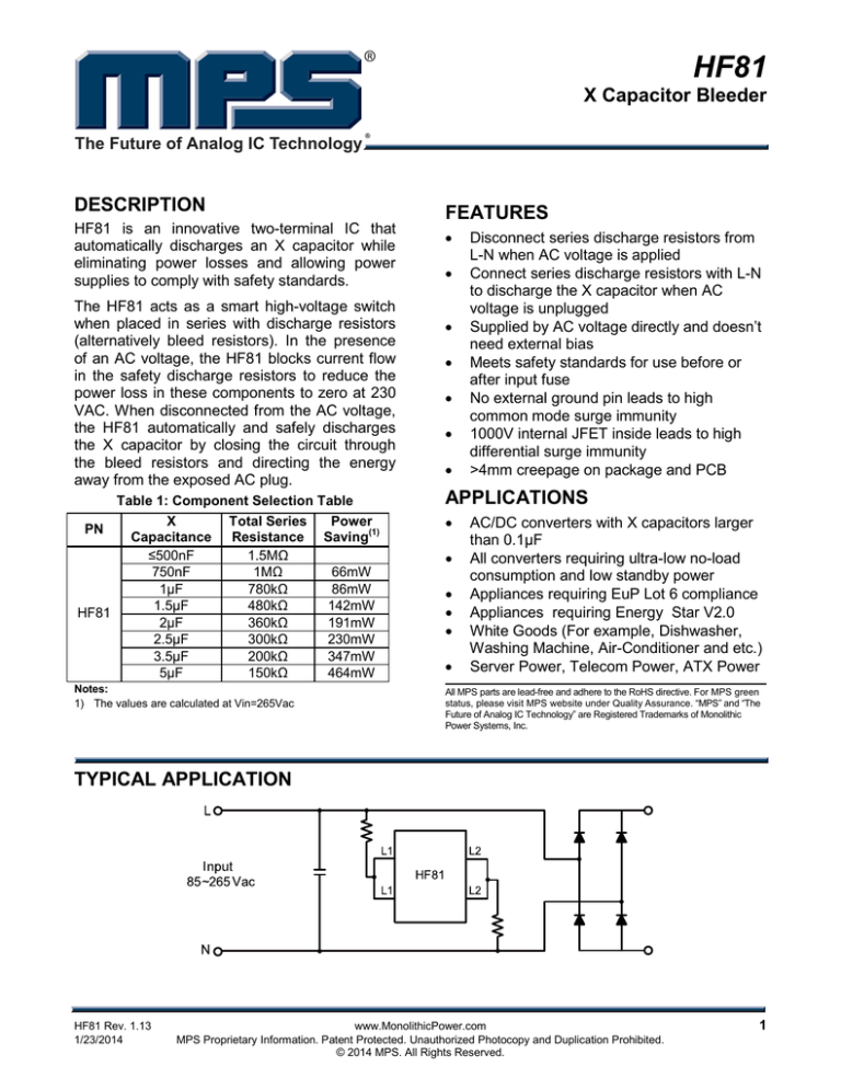
TYPICAL APPLICATION
HF81 Rev. 1.13
1/23/2014
www.MonolithicPower.com
MPS Proprietary Information. Patent Protected. Unauthorized Photocopy and Duplication Prohibited.
© 2014 MPS. All Rights Reserved.
1
HF81 – X CAPACITOR BLEEDER
ORDERING INFORMATION
Part Number*
HF81GS
Package
SOIC8
Top Marking
HF81
* For Tape & Reel, add suffix –Z (e.g. HF81GS–Z);
PACKAGE REFERENCE
TOP VIEW
NC
1
8
NC
L1
2
7
L2
L1
3
6
L2
NC
4
5
NC
ABSOLUTE MAXIMUM RATINGS (2)
Thermal Resistance
L1-L2 Pin Voltage ....................................1000V
Storage Temperature................. -65°C to 150°C
Lead Temperature ................................... 260°C
(3)
Continuous Power Dissipation (TA = +25°C)
………………………………………………...1.4W
(4)
Single Avalanche Energy.......................70μJ
(4)
Avalanche Current ................................ 80mA
Junction Temperature.............................. 150°C
SOIC8 .................................... 90 ...... 45... °C/W
Recommended Operating Conditions
(5)
Operating Junction Temp. (TJ). -40°C to +125°C
HF81 Rev. 1.13
1/23/2014
(6)
θJA
θJC
Notes:
2) Exceeding these ratings may damage the device.
3) The maximum allowable power dissipation is a function of the
maximum junction temperature TJ (MAX), the junction-toambient thermal resistance θJA, and the ambient temperature
TA. The maximum allowable continuous power dissipation at
any ambient temperature is calculated by PD (MAX) = (TJ
(MAX)-TA)/θJA. Exceeding the maximum allowable power
dissipation will cause excessive die temperature, and the
regulator will go into thermal shutdown. Internal thermal
shutdown circuitry protects the device from permanent
damage.
4) L=5mH, Vgs=10V, VDD=1.4V
5) The device is not guaranteed to function outside of its
operating conditions.
6) Measured on JESD51-7, 4-layer PCB.
www.MonolithicPower.com
MPS Proprietary Information. Patent Protected. Unauthorized Photocopy and Duplication Prohibited.
© 2014 MPS. All Rights Reserved.
2
HF81 – X CAPACITOR BLEEDER
ELECTRICAL CHARACTERISTICS
TA = 25°C, unless otherwise noted.
Parameter
AC Removal Detection
Time
(7)
Saturation Current
Supply Current
UVLO
Symbol
Condition
tDETECT
Line Cycle Frequency 47 to 63Hz
ISC
L1-L2 voltage from 110V to 410V
L1-L2 voltage 1000V
ISUPPLY
V_OFF_L1/L2
Min
Typ
Max
Units
25
ms
3.7
mA
μA
V
3.0
15
Notes:
7) Saturation current specifications guarantee natural discharge characteristic at all input voltage with the external resistor and capacitor
specified in Table 1.
HF81 Rev. 1.13
1/23/2014
www.MonolithicPower.com
MPS Proprietary Information. Patent Protected. Unauthorized Photocopy and Duplication Prohibited.
© 2014 MPS. All Rights Reserved.
3
HF81 – X CAPACITOR BLEEDER
TYPICAL CHARACTERISTICS
Leakage Current_1000V
vs. Temperature Chart
Detection Time vs.
Temperature Chart
1000V on L1-L2
L2 connects GND, voltage on L1 is
from -20V to 90V
35
18
16
14
12
10
8
6
4
2
0
-50 -30 -10 10 30 50 70 90 110 130
HF81 Rev. 1.13
1/23/2014
D ETECTIO N T IM E(mS )
20
30
25
20
15
10
5
0
-50 -30 -10 10 30 50 70 90 110130
www.MonolithicPower.com
MPS Proprietary Information. Patent Protected. Unauthorized Photocopy and Duplication Prohibited.
© 2014 MPS. All Rights Reserved.
4
HF81 – X CAPACITOR BLEEDER
PIN FUNCTIONS
Package Pin #
Name
1
2
3
4
5
6
7
NC
L1
L1
NC
NC
L2
L2
Not Connected
AC Line 1
AC Line 1
Not Connected
Not Connected
AC Line 2
AC Line 2
8
NC
Not Connected
HF81 Rev. 1.13
1/23/2014
Description
www.MonolithicPower.com
MPS Proprietary Information. Patent Protected. Unauthorized Photocopy and Duplication Prohibited.
© 2014 MPS. All Rights Reserved.
5
HF81 – X CAPACITOR BLEEDER
OPERATION
A smart bleeder normally works as an off device:
It consumes very little current, it always monitors
the AC line for zero crossings; whenever it
detects a zero crossing it dischargers the timer
capacitor and resets the latch circuit.
Whenever a prolonged period occurs without a
zero crossing (meaning the power supply unit
[PSU] was unplugged from the utility line), the
timer block times out and triggers the latch circuit.
The latch circuit turns on the discharging
transistors, as shown by the timing diagram in
Figure 1. The internal transistor enables the
bleed resistors, and stops when either the
voltage across the HF81 drops below 10V or the
PSU is plugged back into the utility line. This
operation allows for more X capacitor choices
and reduces the inductor cost.
Carefully select a metal oxide varistor (MOV) and
fuse to meet safety requirements: The MOV
suppresses voltage transients. During normal
operation, a MOV with high impedance permits
only a small current. When a voltage surge
occurs, the MOV resistance reduces to a few Ωs,
which allows the large surge current to flow
through while protecting other devices in parallel
to it.
There are several parameters for selecting a
MOV, including maximum-allowable voltage,
maximum clamping voltage, and the MOV max
endured energy. The maximum-allowable voltage
must exceed the maximum working voltage by
10%, 20% or the circuit needs an even higher
derating, which is determined by the power
source stability. After selecting a MOV, verify it
using V1mA, which is the voltage across the MOV
the current is 1mA. Simplified, this is:
V1mA = 1.5Vpeak = 2.2VAC
Zero Crossing
Detection Timing
VXCap
100V/div
22ms
Figure 1: Zero-Crossing Detection Timing
COMPONENT SELECTION
According to international safety requirements,
the X capacitor voltage must drop to 37% within
1s. Based on a 5% tolerance for the discharge
resistor and a 20% tolerance for the X capacitor,
select an RC time constant of 0.75s. Table 1
provides sample values for the X capacitor and
the discharge resistance.
(1)
Where Vpeak is the peak working voltage and VAC
is the rms working voltage.
Also, please make sure the breakdown voltage of
other components on the AC side fall below the
maximum allowable voltage.
Base MOV size selection on MOV withstanding
transient energy. Calculate the energy using
formula 2.
W = K × VClamp × IPeak × t
(2)
Where K is a constant 1.0 for rectangular
waveform and 1.4 for 8/20µs and 10/1000µs
waveform, VClamp is the maximum clamping
voltage, and IPeak is the peak applied current.
Make sure that the calculated energy is lower
than the rated energy on the MOV datasheet.
Select the fuse based on MOV specification.
Generally, select the fuse based on MOV
diameter as per Table 2.
HF81 Rev. 1.13
1/23/2014
www.MonolithicPower.com
MPS Proprietary Information. Patent Protected. Unauthorized Photocopy and Duplication Prohibited.
© 2014 MPS. All Rights Reserved.
6
HF81 – X CAPACITOR BLEEDER
Table 2: Fuse Selection Table
MOV Dimension (mm)
Fuse (A)
Ø5
1-2
Ø7
2-3
Ø10
3-5
Ø14
3-10
Ø20
5-15
Common
Choke
Fuse
R1
MOV
Position 2
MOV
Position 1
AC
OR
X Cap 1
R2
X CAP
BLEEDER
X Cap 2
Differential
Inductor
EMI Inductive Components
Figure 2: HF81 Position Selection
HF81 Rev. 1.13
1/23/2014
www.MonolithicPower.com
MPS Proprietary Information. Patent Protected. Unauthorized Photocopy and Duplication Prohibited.
© 2014 MPS. All Rights Reserved.
7
HF81 – X CAPACITOR BLEEDER
HF81 Position Selection
Figure 2 shows a typical front-end configuration
of offline products. The configuration influences
the position selection for the HF81.
Large currents flow through the MOV whenever a
voltage surge occurs, which can cause significant
voltage drops across inductive EMI components
and traces. Place the HF81 as close as possible
to the MOV.
1. For MOV in position 1, place the HF81
directly underneath the X cap.
2. For MOV in position 2, place the HF81 on the
same side and physically close to MOV. If the
HF81 cannot be placed at the same side as
the MOV, make sure the surge level no
higher than 1.5kV.
3. For surge levels higher than 1.5kV, place the
HF81 and MOV on the same side as the
inductive EMI components.
X capacitor can be placed before the input fuse.
In this case, if the value of the X capacitor
exceeds 0.1μF; to meet safety requirements,
place the HF81 in front of the input fuse. Also,
place the MOV before the input fuse if surge
voltage is >1.5kV.
PCB Layout and Discharge Resistor Selection
Figure 3 shows the typical PCB layout of the
HF81. The discharge resistors are divided into
two separate surface mount resistors. Resistors
R1 and R2 need to be rated for 50% power
dissipation and voltage rating in order to
dissipate loss and withstand the input voltage
under a short between the L1 and L2 terminals of
the HF81.
If the application needs lower power rating or
voltage rating discharge resistor, the discharge
resistor can be divided more discrete resistors
though the total external resistance must be
equal to the values specified in Table 1.
Safety Consideration
To satisfy safety requirements, the HF81 has
double pins for each terminal for design
redundancy. During a single point failure test, if
one pin is physically disconnected to the part or
PCB, the HF81 continues to function normally. If
one pin of part shorts to another at an opposite
terminal, the HF81 shorts and is equivalent to a
system without the HF81, which is also safe.
Table 3 summaries the results of single-point
failure testing. Under open or short conditions,
the HF81 has a null effect on power systems
compared to systems without the HF81.
X Cap
MOV
Figure 3: Typical PCB Layout
HF81 Rev. 1.13
1/23/2014
www.MonolithicPower.com
MPS Proprietary Information. Patent Protected. Unauthorized Photocopy and Duplication Prohibited.
© 2014 MPS. All Rights Reserved.
8
HF81 – X CAPACITOR BLEEDER
Table 3: Single Point of Failure Test
Test
Test with HF81
Test without HF81
R1
ٛ
NC
L1
1
2
3
4
X Capacitor
X Capacitor
AC
8
7
6
5
NC
L2
L2
NC
R2
R2
R1
R1
Open one
pin of HF81
has no
influence of
discharge
function as
two pins at
each side for
redundancy
design.
Short two
NC
L1
L1
NC
1
2
3
4
X Capacitor
AC
X Capacitor
AC
8
L2
NC
L2
R2
7
NC
X CAP
BLEEDER
6
5
HF81 Rev. 1.13
1/23/2014
R1
AC
X CAP
BLEEDER
Short Two
pins
Short any two
pins of
HF81to see if
it can affect
the system
L1
NC
Open One
Pin
Disconnect
any pin of
HF81 to see
it can affect
the system
Comments
R2
www.MonolithicPower.com
MPS Proprietary Information. Patent Protected. Unauthorized Photocopy and Duplication Prohibited.
© 2014 MPS. All Rights Reserved.
pins at
different side
leads to the
circuit
equivalent to
a system
without
HF81.
9
HF81 – X CAPACITOR BLEEDER
PACKAGE INFORMATION
SOIC8
0.189(4.80)
0.197(5.00)
8
0.050(1.27)
0.024(0.61)
5
0.063(1.60)
0.150(3.80)
0.157(4.00)
PIN 1 ID
1
0.228(5.80)
0.244(6.20)
0.213(5.40)
4
TOP VIEW
RECOMMENDED LAND PATTERN
0.053(1.35)
0.069(1.75)
SEATING PLANE
0.004(0.10)
0.010(0.25)
0.013(0.33)
0.020(0.51)
0.0075(0.19)
0.0098(0.25)
SEE DETAIL "A"
0.050(1.27)
BSC
SIDE VIEW
FRONT VIEW
0.010(0.25)
x 45o
0.020(0.50)
GAUGE PLANE
0.010(0.25) BSC
0o-8o
0.016(0.41)
0.050(1.27)
DETAIL "A"
HF81 Rev. 1.13
1/23/2014
NOTE:
1) CONTROL DIMENSION IS IN INCHES. DIMENSION IN
BRACKET IS IN MILLIMETERS.
2) PACKAGE LENGTH DOES NOT INCLUDE MOLD FLASH,
PROTRUSIONS OR GATE BURRS.
3) PACKAGE WIDTH DOES NOT INCLUDE INTERLEAD FLASH
OR PROTRUSIONS.
4) LEAD COPLANARITY (BOTTOM OF LEADS AFTER FORMING)
SHALL BE 0.004" INCHES MAX.
5) DRAWING CONFORMS TO JEDEC MS-012, VARIATION AA.
6) DRAWING IS NOT TO SCALE.
www.MonolithicPower.com
MPS Proprietary Information. Patent Protected. Unauthorized Photocopy and Duplication Prohibited.
© 2014 MPS. All Rights Reserved.
10
Mouser Electronics
Authorized Distributor
Click to View Pricing, Inventory, Delivery & Lifecycle Information:
Monolithic Power Systems (MPS):
HF81GS-LF HF81GS-LF-Z HF81GS HF81GS-Z
