Microwave Filter Design Chp5. Lowpass Filters
advertisement

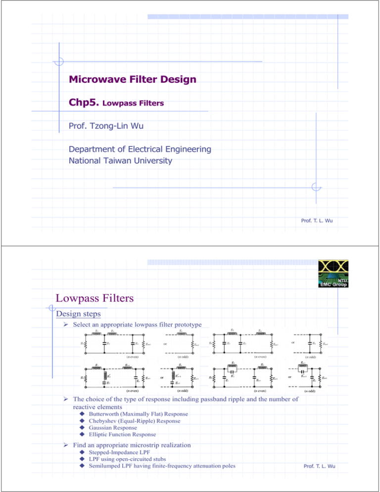
Microwave Filter Design Chp5. Lowpass Filters Prof. Tzong-Lin Wu Department of Electrical Engineering National Taiwan University Prof. T. L. Wu Lowpass Filters Design steps Select an appropriate lowpass filter prototype The choice of the type of response including passband ripple and the number of reactive elements Butterworth (Maximally Flat) Response Chebyshev (Equal-Ripple) Response Gaussian Response Elliptic Function Response Find an appropriate microstrip realization Stepped-Impedance LPF LPF using open-circuited stubs Semilumped LPF having finite-frequency attenuation poles Prof. T. L. Wu Stepped-Impedance LPF General structure – cascaded structure of high- and low-impedance TML Shorter than guided-wavelength Design considerations Z0C < Z0 < Z0L, where Z0C and Z0L denote the characteristic impedances of the low and high impedane lines, respectively, and Z0 is the source impedance, which is usually 50 ohms. Lower Z0C results in a better approximation of a lumped-element capacitor, but the resulting line width WC must not allow any transverse resonance to occur at operation frequency. Higher Z0L leads to a better approximation of a lumped-element inductor, but Z0L must not be so high that its fabrication become difficult, or its current-carrying capability becomes a limitation. Prof. T. L. Wu Example - Stepped-impedance LPF Design a three-order LPF with 0.1 dB ripple and cutoff frequency of 1 GHz. The source/load impedance of the filter is 50 Ω. Step 1 – Find out the required L/C element values Step 2 – Choose the adequate design parameters of microstrip lines fabricated on a substrate with a relative dielectric constant of 10.8 and a thickness of 1.27 mm. Prof. T. L. Wu Example - Stepped-impedance LPF Step 3 – physical length of the high- and low-impedance lines Initial guess for the physical length Compensate the parasitic elements Prof. T. L. Wu Example - Stepped-impedance LPF Step 4 – take discontinuities into account as circuit simulator is used Step Step Step Step Prof. T. L. Wu LPF using open-circuited stubs General structure – high-impedance TML and open-circuited stubs Prof. T. L. Wu Example - LPF with open-circuited stubs Design a three-order LPF with 0.1 dB ripple and cutoff frequency of 1 GHz. The source/load impedance of the filter is 50 Ω. Step 1 – Find out the required L/C element values Step 2 – Choose the adequate design parameters of microstrip lines fabricated on a substrate with a relative dielectric constant of 10.8 and a thickness of 1.27 mm. Prof. T. L. Wu Example - LPF with open-circuited stubs Step 3 –physical length of the high- and low-impedance lines Initial guess for the physical length Compensate the discontinuities 1. parasitic effect on high-impedance line 2. open-end Prof. T. L. Wu Example - Results and comparisons LPF with open-circuited stubs can exhibit a better stopband characteristic. Prof. T. L. Wu Example - LPF with open-circuited stubs To obtain a sharper rate of cutoff, a seven-order LPF is designed with 0.1 dB ripple and cutoff frequency of 1 GHz. The source/load impedance of the filter is 50 Ω. Prof. T. L. Wu LPF with attenuation poles (transmission zeros) To obtain an sharper rate of cutoff, attenuation poles are required to achieve the frequency response. Prototype filter with elliptic function response Attenuation pole General structure – cascaded structure of open-circuited stubs, high- and lowimpedance TML Prof. T. L. Wu Example - LPF with attenuation poles Design a six-order elliptic LPF with a passband ripple LAr = 0.18 dB and a minimum stopband attenuation LAs = 38.1 dB at Ωs = 1.194 for cutoff Ωc = 1. The filter is designed at cutoff frequency fc = 1 GHz and the source/load impedance of the filter is 50 Ω. Step 1 – Find out the required L/C element values Attenuation poles Prof. T. L. Wu Example - LPF with attenuation poles Step 2 – Choose the adequate design parameters of microstrip lines Step 3 – Initial physical length of the high- and low-impedance lines Step 4 – Compensate the parasitic elements 1. For L5 and C6 Prof. T. L. Wu Example - LPF with attenuation poles Step 4 – Compensate the parasitic elements 2. For L2 and C2 or L4 and C4 (fixed ƖL1, ƖL2, and ƖL3) where The same method can be applied to L4 and C4 and the corrected length are ƖL4 = 6.49 mm and ƖC4 = 4.24 mm. 3. ƖC2 and ƖC4 on open-end effect Prof. T. L. Wu Example - LPF with attenuation poles A sharp rate of cutoff with two attenuation poles is designed The unwanted transmission peak could be moved away up to a higher frequency if higher characteristic impedance could be used for the inductive lines. Step 5 – take discontinuities into account T-junction Steps Steps Attenuation poles Prof. T. L. Wu HW II Please design a LPF based on Chebyshev prototype with following specifications: 1. Passband ripple < 0.0432 dB 2. Cutoff frequency : 1 GHz 3. Insertion loss > 30 dB at 3 GHz. The properties of the substrate is FR4 with εr = 4.2 and loss tangent 0.01. The substrate thickness is 1.6 mm. The high and low impedance used in this design is 90 ohm and 25 ohm, respectively. (Note: Please consider the parasitic effects and discontinuities) a. b. c. d. e. Please decide the order of the LPF and calculate the lumped element values of L and C. Based on step impedance approach, please plot the layout of the LPF, and calculate (and denote) the corresponding geometry dimensions. Plot the return loss and insertion loss for the designed LPF using ADS. Simulate the return loss and insertion loss for the designed LPF using full-wave simulator (CST or HFSS), and compare the results with those modeled in (c). Please also discuss the reasons for the discrepancy between them. Based on the open-circuited stubs approach, please repeat steps (b) to (d). Prof. T. L. Wu


