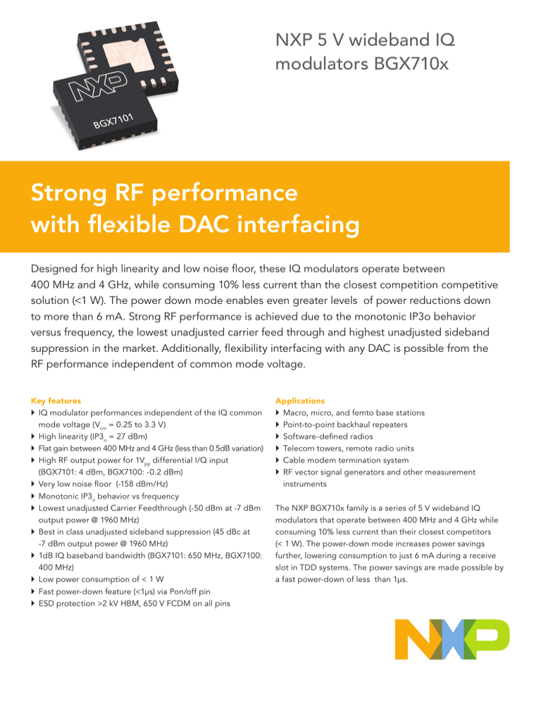
NXP 5 V wideband IQ
modulators BGX710x
Strong RF performance
with flexible DAC interfacing
Designed for high linearity and low noise floor, these IQ modulators operate between
400 MHz and 4 GHz, while consuming 10% less current than the closest competition competitive
solution (<1 W). The power down mode enables even greater levels of power reductions down
to more than 6 mA. Strong RF performance is achieved due to the monotonic IP3o behavior
versus frequency, the lowest unadjusted carrier feed through and highest unadjusted sideband
suppression in the market. Additionally, flexibility interfacing with any DAC is possible from the
RF performance independent of common mode voltage.
Key features
`` IQ modulator performances independent of the IQ common
mode voltage (Vcm = 0.25 to 3.3 V)
`` High linearity (IP3o = 27 dBm)
`` Flat gain between 400 MHz and 4 GHz (less than 0.5dB variation)
`` High RF output power for 1Vpp differential I/Q input
(BGX7101: 4 dBm, BGX7100: -0.2 dBm)
`` Very low noise floor (-158 dBm/Hz)
`` Monotonic IP3o behavior vs frequency
`` Lowest unadjusted Carrier Feedthrough (-50 dBm at -7 dBm
output power @ 1960 MHz)
`` Best in class unadjusted sideband suppression (45 dBc at
-7 dBm output power @ 1960 MHz)
`` 1dB IQ baseband bandwidth (BGX7101: 650 MHz, BGX7100:
400 MHz)
`` Low power consumption of < 1 W
`` Fast power-down feature (<1µs) via Pon/off pin
`` ESD protection >2 kV HBM, 650 V FCDM on all pins
Applications
`` Macro, micro, and femto base stations
`` Point-to-point backhaul repeaters
`` Software-defined radios
`` Telecom towers, remote radio units
`` Cable modem termination system
`` RF vector signal generators and other measurement
instruments
The NXP BGX710x family is a series of 5 V wideband IQ
modulators that operate between 400 MHz and 4 GHz while
consuming 10% less current than their closest competitors
(< 1 W). The power-down mode increases power savings
further, lowering consumption to just 6 mA during a receive
slot in TDD systems. The power savings are made possible by
a fast power-down of less than 1µs.
The devices are designed for high linearity and low noise
floor. Their performance on IP3o behavior versus frequency
is very strong. Where other devices show chaotic output,
these devices are almost flat over the frequency range.
Low unadjusted carrier feedthrough, along with the highest
unadjusted sideband suppression available on the market,
results in very stable operation over the entire temperature
range.
Because their RF performance is independent of common
mode voltage, these modulators offer flexible interfacing with
any DAC. This simplifies design-in, improves performance by
retaining the IQ modulator’s output power, and can lower the
bill of materials.
Typical applications place the IQ modulator as part of the
transmit path of a base station, positioned after the DAC and
before the amplifier. After the signals are fed to the I-DAC and
Q-DAC, they are converted to the analog domain. Before the
I and Q signals enter the IQ modulator, they are first low-pass
filtered through a reconstruction filter to remove any aliasing
signals. At the IQ modulator, the signals are up-converted
to RF using an LO signal coming from the PLL/VCO device,
typically referred to as the LO generator.
Type
Package
Frequency
range (MHz)
Mode Poff
consumption (mA)
Vcc (V)
Icc (mA)
Gain (dB)
Noise Floor
(dBm/Hz)
PL(1dB) (dBm)
IP3o (dBm)
Po 1Vpp differential
(dBm)
Sideband suppression
(dBc)
Carrier
feedthrough
(dBm)
S11_LO
(dB)
Key parameters
BGX7100
SOT616-3
400 - 4000
6
5
175
1.8
-158
11.5
27
-0.2
55
-48
12
BGX7101
SOT616-3
400 - 4000
6
5
178
6
-158
12
27
4
55
-48
12
Typical BGX710x application in the transmit path of a base station
JEDEC Interface
IQ-Modulator
Power Amplifier
I
DVGA RF-BP
PLL
VCO
Dual
DAC
Q
0
MPA
HPA
90
Transmitter
Colored blocks are NXP solutions
Unleash the performance of your RF and microwave designs
www.nxp.com
© 2012 NXP Semiconductors N.V.
All rights reserved. Reproduction in whole or in part is prohibited without the prior written consent of the copyright owner. The
Date of release: October 2012
information presented in this document does not form part of any quotation or contract, is believed to be accurate and reliable and
Document order number: 9397 750 17342
may be changed without notice. No liability will be accepted by the publisher for any consequence of its use. Publication thereof
Printed in the Netherlands
does not convey nor imply any license under patent- or other industrial or intellectual property rights.

![dB = 10 log10 (P2/P1) dB = 20 log10 (V2/V1). dBm = 10 log (P [mW])](http://s2.studylib.net/store/data/018029789_1-223540e33bb385779125528ba7e80596-300x300.png)


