CMOS Processing CMOS Technologies n-well process p
advertisement
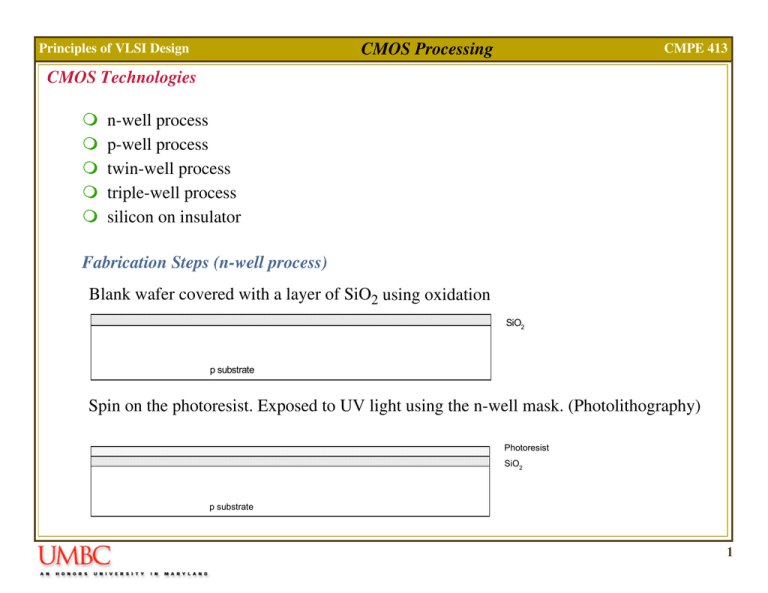
CMOS Processing Principles of VLSI Design CMPE 413 CMOS Technologies n-well process p-well process twin-well process triple-well process silicon on insulator Fabrication Steps (n-well process) Blank wafer covered with a layer of SiO2 using oxidation SiO2 p substrate Spin on the photoresist. Exposed to UV light using the n-well mask. (Photolithography) Photoresist SiO2 p substrate 1 CMOS Processing Principles of VLSI Design CMPE 413 N-Well Process Strip off the exposed photoresist using organic solvents Photoresist SiO2 p substrate Etch the uncovered oxide using HF (Hydroflouric acid) Photoresist SiO2 p substrate Etch the remaining photoresist using a mixture of acids SiO2 p substrate n-well is formed using either diffusion or ion implantation SiO2 n well 2 CMOS Processing Principles of VLSI Design CMPE 413 N-Well Process Strip off remaining oxide using HF. Subsequent steps use the same photolithography process n well p substrate Deposit thin layer of oxide. Use CVD to form poly and dope heavily to increase conductivity Polysilicon Thin gate oxide n well p substrate Pattern poly using the previously discussed photolithography process Polysilicon Thin gate oxide n well p substrate Cover with oxide to define n diffusion regions n well p substrate 3 CMOS Processing Principles of VLSI Design CMPE 413 N-Well Process Pattern oxide using n+ active mask to define n diffusion regions n well p substrate Diffusion or ion implantation used to create n diffusion regions n+ n+ n+ n well p substrate Strip off the oxide to complete patterning step n+ n+ n+ n well p substrate Similar steps used to create p diffusion regions p+ n+ n+ p+ p+ n+ n well p substrate 4 CMOS Processing Principles of VLSI Design CMPE 413 N-Well Process Cover chip with thick field oxide and etch oxide where contact cuts are needed Thick field oxide p+ n+ n+ p+ p+ n+ n well p substrate Remove excess metal leaving wires Metal Masks Thick field oxide p+ n+ n+ p+ p+ n+ Nwell n well p substrate Layout (mask) view of the inverter. poly N+ A P+ Y contacts GND VDD nMOS transistor substrate tap metal 1 pMOS transistor well tap 5 Principles of VLSI Design CMOS Processing CMPE 413 Design Rules Main objective of design rules is to build reliably functional circuits in as small an area as possible. They represent a compromise between performance and yield More conservative rules increase probability of correct circuit function More aggressive rules increase circuit performance Two approaches used Lambda based rules: Also known as scalable rules as they allow first order scaling Moving from one process to another requires only a change in λ. Worked well for 4µm down to 1.2 µm processes. In general, process rarely shrinks uniformly. Micron based rules: All minimum sizes and spacings specified in microns. Rules don't have to be multiples of λ. Can result in 50% reduction in area over λ based rules Standard in industry. 6 Principles of VLSI Design CMOS Processing CMPE 413 Manufacturing Issues and related rules Antenna Rules: Specify maximum area of metal that can be connected to a gate When metal wire contacted to transistor gate is plasma etched, it can charge up to a sufficient voltage to break down thin gate oxides. Metal can be contacted to diffusion to provide a path for the charge to bleed away. Violations can be fixed by using diffusion diodes or by shortening the metal segments. Layer Density Rules: Specify minimum and maximum density of particular layer within a specified area. Required to achieve uniform etch rates when using the CMP process. For e.g. a metal layer might have a 30% minimum and 70% maximum fill with a 1mm by 1mm area. Resolution Enhancement Rules: Some resolution enhancement techniques discussed before impose additional rules For e.g. polysilicon gates should be drawn in a single orientation (horizontal or vertical) Modern design tools, can check for rules violations and also fix most of them automatically. 7 Principles of VLSI Design CMOS Processing CMPE 413 CMOS Process Enhancements Transistors Multiple threshold voltages and oxide thicknesses Processes offer multiple threshold voltages Low threshold devices: faster, higher leakage. High threshold devices: opposite Thin oxides: provide high ON currents but cannot handle high voltages (e.g. I/Os) Thicker oxides provided for I/O devices Silicon on Insulator As the name suggests transistors are fabricated on an insulator (SiO2 or sapphire) Insulating substrate eliminates capacitance between the source/drain and body, higher speed devices and low leakage currents. N transistor P transistor N transistor P transistor n+ p n+ p+ n p+ Sapphire n+ p n+ p+ n p+ Buried Silicon Oxide (BOX) Substrate 8 Principles of VLSI Design CMOS Processing CMPE 413 CMOS Process Enhancements Transistors (contd.) High-k gate dielectrics Transistors need high gate capacitance to attract charge to the channel Thin gates and therefore high gate leakages Thicker gates that leak less can be made with high-k materials e.g. hafnium oxide (k=20), zirconium oxide (k=23), silicon nitride (k=6.5-7.5) Applied using ALD, MOCVD (metallo-organic CVD) or sputtering. Low leakage transistors Scaling transistors causes exponential increase in subthreshold leakages Can be improved using gate structure where gates is placed on more than one side of the channel gate oxide These devices are generically called finfets Width is defined by the height of the fin. 9 Principles of VLSI Design CMOS Processing CMPE 413 CMOS Process Enhancements Transistors (contd.) Higher mobility Achieved by using SiGe (silicon germanium) for bipolar transistors in the same conventional CMOS process Silicon Germanium can also be used to improve speed by creating strained silicon Plastic transistors MOS transistors fabricated with organic chemicals Used only for very specific applications as devices are very inexpensive to manufacture High-voltage transistors High voltage MOSFETs can be integrated onto conventional CMOS processes for switching and high-power applications. Specialized process steps required to achieve very high breakdown voltages. 10 Principles of VLSI Design CMOS Processing CMPE 413 CMOS process Enhancements Interconnect Copper Damascene process Using copper (higher conductivity) as interconnect instead of aluminum. Several challenges due to copper atom diffusion, etching issues and copper oxide formation. Special barrier layers used to prevent copper from entering the silicon surface. New metallization process called Damascene process invented to form barrier. Subtractive aluminum based metallization step involved adding aluminum everywhere and then etching it away leaving behind wires. Copper metallization is additive, trenches are made and then filled with copper. Conductive Ta or TaN film Copper Etch stop 11 Principles of VLSI Design CMOS Processing CMPE 413 CMOS process Enhancements Interconnect (contd.) Low-k Dielectrics Low-k dielectrics between wires are attractive as they decrease wire capacitance. Reduces wire delay and power consumption. 130nm process uses fluorosilicate glass (FSG, flourine added to silicon dioxide). Other materials have been developed, active research area. Circuit Elements Increasing use of CMOS for mixed signal and RF designs, requires special circuit elements with good characteristics Capacitors In conventional CMOS, capacitors can be created using the gate and source/drain, a diffusion area (to ground or VDD) or a parallel metal plate capacitor. Enhancements include addition of a second polysilicon layer. Other enhanced types include metal-insulator-metal (MiM) capacitor and fringe (fractal) capacitor. 12 Principles of VLSI Design CMOS Processing CMPE 413 CMOS process Enhancements Circuit Elements (contd.) Resistors In conventional CMOS, resistors can be built from any layer, where the final resistance depends on the resistivity (resistance per unit area) of the layer. Large resistance in small areas built using poly or diffusion. However, poly is usually doped so undoped poly allowed in enhanced processes. Another enhancement that requires additional processing steps is to allow nichrome that produces high quality resistors. Inductors Most common monolithic inductor is the spiral inductor, which is a spiral of upper-level metal. Used mainly for RF designs. Several enhancements techniques used to increase Q (self-resonant frequency). Other elements Other enhancements allow transmission lines, non-volatile memory, bipolar transistors, fuses and antifuses and micro electro mechanical systems (MEMS). Nanotechnology is considered the CMOS replacement in future, When and What??? 13

