Digital Logic Basics
advertisement
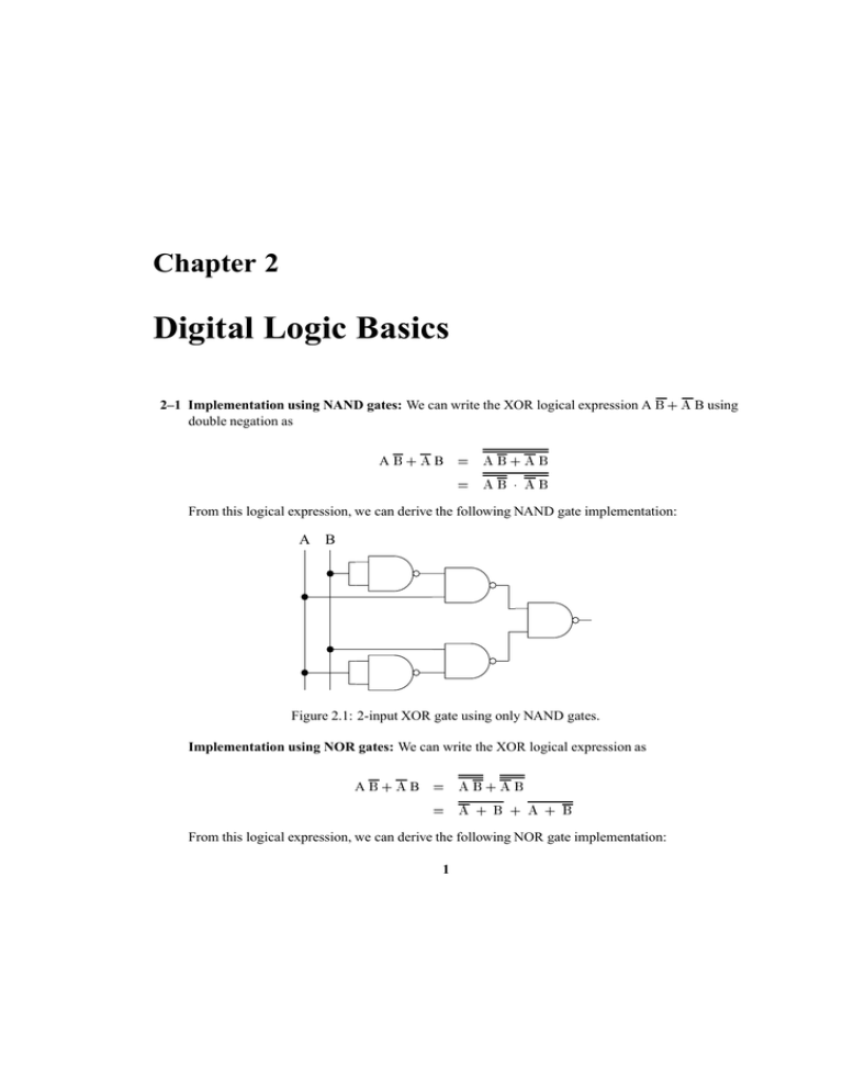
Chapter 2 Digital Logic Basics 2–1 Implementation using NAND gates: We can write the XOR logical expression A B + A B using double negation as AB+AB = AB+AB = AB AB From this logical expression, we can derive the following NAND gate implementation: A B Figure 2.1: 2-input XOR gate using only NAND gates. Implementation using NOR gates: We can write the XOR logical expression as AB+AB = AB+AB = A + B + A + B From this logical expression, we can derive the following NOR gate implementation: 1 2 Chapter 2 A B Figure 2.2: 2-input XOR gate using only NOR gates. 2–2 Implementation using NAND gates: We can write the exclusive-NOR logical expression A B + A B using double negation as AB+A B = AB + AB = AB AB From this logical expression, we can derive the following NAND gate implementation: A B 3 Chapter 2 Implementation using NOR gates: We can write the exclusive-NOR logical expression as AB+A B = AB+AB = A + B + A + B From this logical expression, we can derive the following NOR gate implementation: A B Alternative Implementations: Alternatively, we can derive the following NAND implementation by modifying the logic circuit in Figure 2.1 by adding an output inverter: A B 4 Chapter 2 Similarly, we derive the following NOR implementation by modifying the logic circuit in Figure 2.2 by deleting the output inverter: A B 2–3 A NOT gate can be implemented by holding one input at ‘1’ as shown below: 1 A A 2–4 By keeping one input at ‘0’, we can turn an XOR gate into a buffer that passes input to output as shown below: A A It is clear from this and the last exercise that by controlling one input (call it control input), we can turn an XOR gate into either an inverter or a buffer. If the control input is ‘1’, the XOR gate acts as an inverter; if the control input is ‘0’, it acts as a buffer. 2–5 We can write the AND logical expression (A B) using double negation as AB = AB = A + B From this logical expression, we can derive the following implementation: 5 Chapter 2 A B 2–6 We can write the OR logical expression (A + B) using double negation as A + B = A + B = A B From this logical expression, we can derive the following implementation: A B 2–7 The two transistors are in series. V out is low only when both transistors are turned on. This happens only when both V in1 and Vin2 are high as shown below: Vin1 low low high high Vin2 low high low high Vout high high high low As in the text, when we interpret low as ‘0’ and high as ‘1’, it implements the NAND function. 2–8 In this example, the two transistors are in parallel. V out is low when any of the two transistors are turned on. This happens when either V in1 or Vin2 (or both) is high as shown below: Vin1 low low high high Vin2 low high low high Vout high low low low As in the text, when we interpret low as ‘0’ and high as ‘1’, it implements the NOR function. 2–9 We assume that input A has 50% weight. The truth table is shown below: 6 Chapter 2 A 0 0 0 0 1 1 1 1 B 0 0 1 1 0 0 1 1 C 0 1 0 1 0 1 0 1 F 0 0 0 1 1 1 1 1 We use the Karnaugh map to derive the simplified logical expression. BC BC A 00 01 11 10 0 0 0 1 0 1 1 1 1 1 A From this K-map, we get the following logical expression: A + BC The following logic circuit implements this function: A B C 2–10 We assume that input A has the veto power. The truth table is shown below: A 0 0 0 0 1 1 1 1 B 0 0 1 1 0 0 1 1 C 0 1 0 1 0 1 0 1 F 0 0 0 0 0 1 1 1 7 Chapter 2 The sum-of-products expression for F can be simplified by replicating the term (A B C) as shown below: F = ABC + ABC + ABC = ABC + ABC + ABC = AC = A(B + C) + + ABC AB You can also use the Karnaugh map method to derive the same logical expression. The following logic circuit implements this function: A B C 2–11 (a) x x = x Let us start with x and show that it is equivalent to x x. x = = = = = x1 Identity) x (x + x) (Complement) (Distribution) (x x) + (x x) (x x) + 0 (Complement) x x (Identity ) ( (b) x + x = x Let us start with x and show that it is equivalent to x + x (very similar to the last exercise). x = = = = = Identity) x + (x x) (Complement) (x + x) (x + x) (Distribution) (x + x) 1 (Complement) x + x (Identity ) x+0 ( (c) x 0 = 0 As in the previous examples, we start with the right hand side (0) and show that it is equivalent to 8 Chapter 2 x 0. xx Complement) x (x + 0) (Identity ) (x x) + (x 0) (Distribution) 0 + (x 0) (Complement) x 0 (Identity ) = 0 = = = = ( (d) x + 1 = 1 This is the dual of the last exercise. Complement) = x + (x 1) (Identity ) = (x + x) (x + 1) (Distribution) (Complement) = 1 (x + 1) = x + 1 (Identity ) (x + y) = 0 and (x y) + (x + y) = 1. = 1 2–12 We have to show (x y) x (x (x 2–13 We have to show (x y) + y) + x y) (x + y) + (x + y) ( y) xyx + = 0 + 0 = 0 xyy = xy + x (y + y) + y (x + x) = xy + x = (x y + x y) + (x y + y x) = (x y + x y) + (x y + y x) = y + y = 1 (x y) = 0 (x + = and (x (x y) + y+ y) xy + y x+yx + (x y) = 1. = xxy + = 0 + 0 = 0 yxy 9 Chapter 2 (x + y) + (x y) = x( y + y) + = xy = x(y = x = 1 + y (x + x) xy+yx + y + + y) + yx + (x y) + xy x (y + y) + x 2–14 AND version: A B C = A + B + C The truth table below verifies the AND version. A 0 0 0 0 1 1 1 1 B 0 0 1 1 0 0 1 1 C 0 1 0 1 0 1 0 1 A B C A + B + C 1 1 1 1 1 1 1 0 1 1 1 1 1 1 1 0 OR version: A + B + C = A B C The truth table below verifies the OR version. A 0 0 0 0 1 1 1 1 B 0 0 1 1 0 0 1 1 C 0 1 0 1 0 1 0 1 A + B + C 1 0 0 0 0 0 0 0 A B C 1 0 0 0 0 0 0 0 2–15 From the 3-input NAND gate shown in Figure 2.23b, we can see that each additional input needs an inverter and a 2-input NAND gate. Since we implement the inverter with a 2-input NAND gate as well, we need two 2-input NAND gates for each additional input. Thus, for an n input NAND gate, we need 1 + 2( n 2) 10 Chapter 2 2-input NAND gates. To build an 8-input NAND gate we need 1 + 2(8 2) = 13 gates Since there are four gates in the 7400 chip, we need four 7400 chips. 2–16 (a) (x + y) (x + y) = (x = 0 y) xy (de Morgon’s law) (b) x + yx = x (1 + y) = x + xy = x + y (x = x + y + + yx yx + x) (c) AB AB = (A + B) (A + B) = AA + AB = A + AB B + BA + BB 2–17 Truth table: A 0 0 0 0 1 1 1 1 B 0 0 1 1 0 0 1 1 C 0 1 0 1 0 1 0 1 F 1 0 0 1 0 1 1 0 Sum-of-products form: ABC + A BC + ABC + ABC Product-of-sums form: (A + B + C) (A + B + C) (A + B + C) (A + B + C) 11 Chapter 2 2–18 We start with the product-of-sums expression and derive the sum-of-products expression. (A + + C) (A + B + B = (A + A B + A = (A C) (A + + B C) (A + B + C) C + A B + B C + A C + B C) (A + B + C) (A + B + C) B C + A B C + A B + A B C + B C + A B C + A C + A B C) (A + B + C) =ABC + A BC + ABC + ABC 2–19 Logic expression for Figure 2.10a is (A B). Logic expression for Figure 2.10b is A + B. We show that this expression is equivalent to (A B). A + B= AB (de Morgon’s law) 2–20 We start with the product-of-sum expression and derive the other expression. (A + B + C ) (A + B + C) (A + B + C) (A + B + C) = (A + A B + A C + B + B C + A C + B C) (A + B + C) (A + B + C) = (A + A B + A C + A B C + A C + A B C + A B + A B C + A B C + B C) (A + B + C) =A BC + + AB By observing that A B products expression. + + ABC + ABC ABC BC + + BC + AC + ABC A C is equivalent to (A B C), we derive the sum-of- 2–21 We start with the product-of-sums expression and derive the sum-of-products expression. (A + B + C) (A + B + C) (A + = (A + A B + A C + A = (A + C) (A + B + B C) B + B C + A C + B C) (A + B + C) (A + B + C) B C + A B C + A B + A B C + B C + A B C + A C + A B C) (A + B + C) =AB C + A BC + ABC + ABC 2–22 Replace the exercise in the book by the following: Using Boolean algebra show that the following two expressions are equivalent: ABC A + A CD + BD + + AB CD + B C C + ABD + + BCD ABC + AC + A BCD 12 Chapter 2 Solution: ABC + = ABC A C (B + A + = (A C + = A + A B) CD + A A C) CD + AB CD A (1 + + A + CD + B C A (1 + ABD + + AB + A ABD + = CD C C + AB C D) + A BCD AC + A + ABD + C + ABD + A + AB C + B D) + A + BD + AC + BCD A (1 + B C) + A (1 + BCD BCD + B C D) BCD 2–23 The logic circuit is shown below: 2–24 We need a 7-input XOR gate to derive the parity bit. We can construct 1 7-input XOR using 2-input XOR gates as shown below: A0 A1 A2 A3 A4 A5 A6 We need to add an inverter at the output to generate odd parity bit. P 13 Chapter 2 2–25 BD + ACD + ABD = B D (1 + A C) + = BD + BD = BD + A B C (D + D) + = BD + ABC ABD AC A C D (B + + + B) + ABCD + ABD ABCD A B D (1 + ABD + C) 2–26 The truth table is shown below: A 0 0 0 0 1 1 1 1 ABC + A BC + ABC + B 0 0 1 1 0 0 1 1 ABC C 0 1 0 1 0 1 0 1 F 1 0 1 0 1 0 1 0 = A C(B + = C(A + = C B) + A C(B A) Clearly, we just need one inverter to implement this simplified logical expression. 2–27 The truth table is shown below: + B) 14 Chapter 2 A 0 0 0 0 0 0 0 0 1 1 1 1 1 1 1 1 B 0 0 0 0 1 1 1 1 0 0 0 0 1 1 1 1 C 0 0 1 1 0 0 1 1 0 0 1 1 0 0 1 1 D 0 1 0 1 0 1 0 1 0 1 0 1 0 1 0 1 F 1 0 0 0 1 0 0 0 1 0 0 0 1 0 0 0 00 01 11 10 00 1 0 0 0 01 1 0 0 0 11 1 0 0 0 10 1 0 0 0 From the following Karnaugh map CD AB CD we get the simplified logical expression as (C D). We just need a single NOR gate to implement this. 2–28 The following table finds the prime implicants: Column 1 ABCD A BCD ABCD ABCD p p p p Column 2 ACD BCD BCD ACD p p p p Column 3 CD 15 Chapter 2 There is no need for Step 2. The simplified expression is C D. 2–29 The truth table is shown below: A 0 0 0 0 0 0 0 0 1 1 1 1 1 1 1 1 B 0 0 0 0 1 1 1 1 0 0 0 0 1 1 1 1 C 0 0 1 1 0 0 1 1 0 0 1 1 0 0 1 1 D 0 1 0 1 0 1 0 1 0 1 0 1 0 1 0 1 F 0 0 0 0 0 1 1 1 1 1 1 0 0 0 0 0 00 01 11 10 00 0 0 0 0 01 0 1 1 1 11 0 0 0 0 10 1 1 0 1 + A BC From the following Karnaugh map CD AB we derive the simplified expression as ABD + ABC + A BD = A B (C The following circuit implements this logic expression: + D) + A B (C + D) 16 Chapter 2 A B C D A B C D 2–30 The following table finds the prime implicants: Column 1 — ABCD A BCD A BCD ABCD ABCD A BCD Column 2 ABD p p p p p p ABC A BD A BC Step 2: Prime implicants ABD A BC A BD AB C Input product terms ABCD ABCD N ABCD ABCD N N ABCD N ABCD 17 Chapter 2 The minimal expression is ABD + ABC + A BD + A BC = A B (C + D) + A B (C + D) 2–31 The truth table is shown below: A 0 0 0 0 0 0 0 0 1 1 1 1 1 1 1 1 B 0 0 0 0 1 1 1 1 0 0 0 0 1 1 1 1 C 0 0 1 1 0 0 1 1 0 0 1 1 0 0 1 1 D 0 1 0 1 0 1 0 1 0 1 0 1 0 1 0 1 F 0 0 1 0 1 1 0 0 0 0 0 1 1 0 1 0 00 01 11 10 00 0 0 0 1 01 1 1 0 0 11 1 0 0 1 10 0 0 1 0 From the following Karnaugh map CD AB we derive the following simplified logic expression: AB CD + ABCD + A BC + ABD = B C (A D An implementation of this logic expression is shown below: + A D) + A BC + ABD 18 Chapter 2 B B A C A D B C A D 2–32 The following table finds the prime implicants: Column 1 Column 2 — AB — CD A BCD A BCD ABCD ABCD ABCD A BC BCD p p p ABD p Step 2: Prime implicants Input product terms ABCD ABC BCD A BD A BCD ABCD ABCD N ABCD N ABCD ABCD ABCD N N 19 Chapter 2 We derive the following simplified logic expression: AB CD + ABCD + A BC + ABD = B C (A D + A D) + A BC + ABD
