4 Digit LCD Data Display Module
advertisement

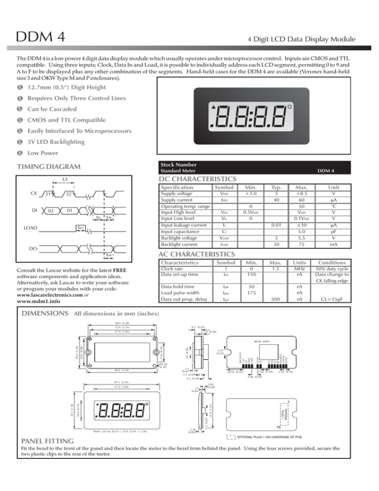
DDM 4 4 Digit LCD Data Display Module The DDM 4 is a low power 4 digit data display module which usually operates under microprocessor control. Inputs are CMOS and TTL compatible. Using three inputs; Clock, Data In and Load, it is possible to individually address each LCD segment, permitting 0 to 9 and A to F to be displayed plus any other combination of the segments. Hand-held cases for the DDM 4 are available (Veronex hand-held size 3 and OKW Type M and P enclosures). 12.7mm (0.5“) Digit Height Requires Only Three Control Lines Can be Cascaded CMOS and TTL Compatible Easily Interfaced To Microprocessors 5V LED Backlighting Low Power Stock Number TIMING DIAGRAM Standard Meter DDM 4 DC CHARACTERISTICS 1/f Specification CK DI 31 02 01 tds tdh tpw LOAD Symbol Min. Typ. Max. Unit VDD IDD +3.0 5 40 +8.5 60 50 VDD 0.1VDD ±10 5.0 5.5 75 V mA °C V V mA pF V mA Supply voltage Supply current Operating temp. range Input High level Input Low level Input leakage current Input capacitance Backlight voltage Backlight current 32 DO 0 0.5VDD 0 VIH VIL IL CI VLMP ILMP 0.01 5 50 AC CHARACTERISTICS tpd Consult the Lascar website for the latest FREE software components and application ideas. Alternatively, ask Lascar to write your software or program your modules with your code. www.lascarelectronics.com or www.mdm1.info Characteristics Symbol Min. Max. Units Conditions Clock rate Data set-up time f 1.5 tds 0 150 MHz nS 50% duty cycle Data change to CK falling edge Data hold time Load pulse width Data out prop. delay tdh tpw tpd 50 175 nS nS nS 500 CL=55pF DIMENSIONS All dimensions in mm (inches) 58.0 (2.28) 6.1 (0.24) 55.0 (2.16) 47.0 (1.85) 1.6 (0.06) 1.5 (0.05) 2.1 (0.08) 4.5 (0.18) 64.5 (2.54) DI DO L0 BP DEGREES COLON POINT 2.00 (0.08) 1 31.8 (1.25) 2.50 (0.09) 5.2 (0.20) 34.5 (1.36) 2.54 (0.10) OPTIONAL PLUG 1 Panel cut-out 62.0 x 32.0 (2.44 x 1.26) PANEL FITTING 1.0 (0.04) 7.62 (0.30) 5.08 (0.20) 18.0 (0.70) 47.0 (1.84) 10.92 (0.43) LOAD CK 5.59 (0.22) BACKLIGHT +VE -VE VPOS VNEG Ø2.50 (0.10) 60.0 (2.36) 5.0 (0.20) 17.8 (0.70) 30.0 (1.18) 25.0 (0.98) REAR VIEW 16 OPTIONAL PLUG 1 ON UNDERSIDE OF PCB Fit the bezel to the front of the panel and then locate the meter to the bezel from behind the panel. Using the four screws provided, secure the two plastic clips to the rear of the meter. LASCAR ELECTRONICS LTD. LASCAR ELECTRONICS INC. LASCAR ELECTRONICS (HK) LTD. MODULE HOUSE, WHITEPARISH, WILTSHIRE SP5 2SJ UK TEL: +44 (0)1794 884567 FAX: +44 (0)1794 884616 E-mail: sales@lascar.co.uk 4258 WEST 12th STREET, ERIE, PA 16505 USA TEL: +1 (814) 835 0621 FAX: +1 (814) 838 8141 E-mail: us-sales@lascarelectronics.com 8th FLOOR, CHINA AEROSPACE CENTRE, 143 HOI BUN ROAD, KWUN TONG, KOWLOON, HONG KONG TEL: +852 2389 6502 FAX: +852 2389 6535 E-mail: saleshk@lascar.com.hk PIN FUNCTIONS (15) (16) (2) (1) (3) (4) (5) (6) -VE +VE VPOS VNEG LOAD CK DI DO (7) (8) (9) (10) (11) L0 BP DEGREES COLON POINT 5 Volt LED backlighting supply terminals. Positive supply voltage (VDD). Negative supply voltage (VSS). Load input: Causes a parallel load of the data from the shift register to the display latches at logic '1'. Clock input: The shift register loads, shifts and outputs (DO) on the falling edge. Data input: A logic '1' on DI causes a segment to be visible. Data output: To be used for cascading modules. For cascading: Connect DO to DI of next module. Each module will produce its own display drive. If an external driving signal is used, connect it to each module's L0 input. Note: Do not connect backplane outputs together. LCD driving signal input. Leave open circuit or use for synchronising cascaded modules (see Application diagram *). Backplane output. Inputs for degree, colon and pointer. Note: If not used, tie these inputs to BP. ( ) Optional Plug 1 Pin Numbers APPLICATION DIAGRAM LOAD LOAD CK CK DI CK TO ADDITIONAL CASCADING MODULES LOAD DI DO DI DRIVE CIRCUIT FOR POINTER, COLON & DEGREES Connect to VPOS to display required symbol CK LOAD DO DI BP L0 VPOS VNEG DDM 4 DDM 4 +VE POINTER BP -VE POINT COLON DEGREES L0 COLON L0 DEGREES OPTIONAL EXTRA MODULE(S) * * NOT PRESENT ON DDM 4 MODULE OPERATION SEE 'TERMINAL DEFINITIONS' Data is clocked into the internal shift register (DI) on the falling edge of the clock (CK). After 32 bits have been clocked in, setting Load to Logic 1 will cause the contents of the register to be displayed on the LCD. If Load is kept at Logic 1, then the shift register becomes transparent. Any new data that is clocked in will be immediately reflected on the display. DISPLAY SHIFT REGISTER ASSIGNMENT Note: A segment is visible when a logic '1' is present. For correct operation of the display, 32 bits of data must be clocked in. When clocking in 32 bits of display data the first input bit is the DP of digit 1 and the last bit is the G segment of digit 4. DIGIT DIGIT 4 'MSD' (LH digit) A F E DP G D B C DIGIT 3 CLOCK PULSE 1 2 3 4 5 6 7 8 9 10 11 12 13 14 15 16 Specifications liable to change without prior warning SEGMENT G F A B C D E DP G F A B C D E DP DDM4 DIGIT DIGIT 2 DIGIT 1 'LSD' (RH digit) Issue 9 06/2010 CLOCK PULSE 17 18 19 20 21 22 23 24 25 26 27 28 29 30 31 32 S.L. SEGMENT G F A B C D E DP G F A B C D E DP Applies to DDM 4/3

