Automotive Electronics
Product Information
Interface for Ignition Drivers – CK110
Customer benefits:
Excellent system know-how
Smart concepts for system safety
Secured supply
Long- term availability of manufacturing processes
and products
QS9000 and ISO/TS16949 certified
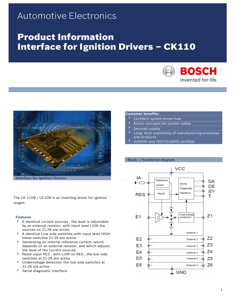
Block- / functional diagram
Interface for Ignition Drivers
.
The CK 110B / UC10B is an inverting driver for ignition
stages.
Features
6 identical current sources , the level is adjustable
by an external resistor, with input level LOW the
sources on Z1-Z6 are active
6 identical Low side switches with input level HIGH
these switches Z1-Z6 are active
Generating an internal reference current, which
depends on an external resistor, and which adjusts
the level of the current sources
Reset input RES , with LOW on RES , the low side
switches at Z1-Z6 are active
Undervoltage detection the low side switches at
Z1-Z6 are active
Serial diagnostic interface
1
The maximum current level of the low side switch is
Maximum ratings
fixed (typ. 45mA).
Parameter
Min
Max
Unit
Junction temperature TJ
Storage temperature TC
Maximal ambient temperature:
TUmax = TJmax - (PV * RTHJC)
with
RTHJC = 85K/W
PV = VCC * IVCC
+(VCC-UZ1) * Isource + UZ1 * Isink
+ ...
+(VCC-UZ6) * Isource + UZ6 * Isink
(Per channel only Isource or Isink is
Power supply static VCC
for maximal one hour in lifetime
Maximal voltage at the driver
outputs UZAi
(without influence to other
channels or to diagnosis)
static
dynamic ( t < 10ms )
-40
-55
150
125
°C
°C
Because of the power consumption this current will be
reduced at short circuit to UBAT ( typ. 2.8mA).
With the input RES the low side switches of all driver
outputs are activated.
active)
0
5.5
5.5
6.5
V
V
Ei
Res
Outputs Zi
X
O
low side switch active
O
1
source active
1
1
low side switch active
X : can be 0 or 1
The inputs E1-E6 and RES include internal pull up
current sources.
-2
-5
Limit for TRISTATE VCC
18
18
V
V
>3
V
An
undervoltage
detection
activates
all
low
side
switches if the power supply voltage is less than typ.
3,8V (hysteresis typ. 50mV).
At a power supply voltage less than max. 3V the outputs
can have a high impedance state.
Functional description
Serial diagnostic interface
Driver for ignition stages
The CK110B / UC10B includes a diagnostic circuit for
The CK110B / UC10B is an interface between processor
(KSM) short circuit to UBAT (KSUB) and open load(LA).
and ignition stages.
6 driver outputs can be controlled by 6 inputs.
With input level LOW a current source is activated, with
input level HIGH a low side switch is activated.
It’s possible to activate more than 1 driver at the same
each channel which detects short circuit to ground
The detection works only when the current source is
activated. When the low side switch is activated no
diagnosis is possible.
If an error occurs the first time an internal counter is
time.
started. The error states of the different channels are
Within the maximum ratings the circuit includes a short
and can be read out with the serial interface.
circuit protection to UBAT and to ground.
At the outputs a maximum capacitance of 10nF is
stored after the delay time in an internal shift register
If there is a change of error condition the internal shift
register will be updated directly without a delay time.
allowed (47nF R = 30Ω).
An error state in the shift register is indicated with a
The current level of all sources is adjustable by an
If a failure has been stored in the shift register and the
external resistor at pin IA to ground.
The dependency is:
LOW on the interface output DA (only when SY is HIGH).
failure condition disappears the last detected failure
remains stored.
Isource = (VCC*100V)/(RIA *5V) 4.5kΩ < RIA < 30kΩ
2
If the SY-signal is LOW the different diagnostic bits can
PIN configuration
be read out with an external clock at pin T.
Each channel has 2 bits in the shift register where the 3
Package: SOIC20L
possible error states can be indicated.
For the 6 channels 12 bits are needed. To have an easier
software for the processor the number of bits in the
shift register is 16. The fixed level of the 4 unneeded
bits is HIGH.
After the transmission the shift register will be reset
with the change of the SY signal from LOW to HIGH. A
new error entry is possible after the delay time when the
error condition occurs.
It’s possible to cascade the diagnostic interface. Also in
this case the DA output changes to LOW when there is
an error entry in any shift register (SY is HIGH).
The output DA of the diagnostic interface is an open
drain output.
The input DE has a pull up current source.
Logic table of the diagnostic interface
R
SY
DE
T
DA
L
H
H
X
H
L
H
L
X
L
L
L
X
X
H
H
H
H
H
H
L
L
H
X
X
X
L
L
H/L
H/L
Pin description SOIC20L
Shift register
Pin
Description
reset, no diagnosis
possible
reset, no diagnosis
possible
reset, no diagnosis
possible
error entry possible
error entry possible
1.Bit on DA , with clock on
T it’s possi-ble to read the
shift register, no error
entry possible
E1 to E6
Z1 to Z6
RES
Inputs to switch the driver
Driver outputs
Reset active with LOW
External resistor to adjust the current source
level
IA
DA , DE ,
T , SY
VCC
GND
Pins for serial diagnostic interface
Power supply 5V
Ground
Contact
Robert Bosch GmbH
Sales Semiconductors
Postbox 13 42
72703 Reutlingen
Germany
Tel.: +49 7121 35-2979
Fax: +49 7121 35-2170
Robert Bosch Corporation
Component Sales
38000 Hills Tech Drive
Farmington Hills, MI 48331
USA
Tel.: +1 248 876-7441
Fax: +1 248 848-2818
E-Mail: bosch.semiconductors@de.bosch.com
Robert Bosch K.K.
Component Sales
9-1, Ushikubo 3-chome
Tsuzuki-ku, Yokohama 224
Japan
Tel.: +81 45 9 12-83 01
Fax: +81 45 9 12-95 73
Internet: www.bosch-semiconductors.de
© 02/2006 All rights reserved by Robert Bosch GmbH including the right to file industrial property rights
Robert Bosch GmbH retains the sole powers of distribution, such as reproduction, copying and distribution.
For any use of products outside the released application, specified environments or installation conditions no warranty shall apply and
Bosch shall not be liable for such products or any damage caused by such products.
3


