Superconducting energy gap of niobium nitride
advertisement

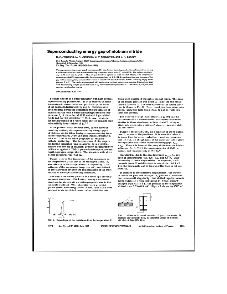
Superconducting energy gap of niobium nitride E. A. Antonova, D. R. Dzhuraev, G. P. Motulevich, and V. A. Sukhov P. N Lebedev Physics Institute, USSR Academy of Sciences and Moscow Institute of Steel and Alloys (Submitted 10 December 1980) Zh. Eksp. Teor. Fiz. 80,24262429 (June 1981) The superconducting energy gap A was measured by the electron tunneling method in niobium nitride having a columnar structure and a superconducting transition temperature T, = 16.15 K. The values obtained, A , = 2.46 meV and 24 dkT, = 3.53, are practically in agreement with the BCS theory. The temperature dependence of A (T)was measured in the temperature interval 2-6.5 K. It was found that the decrease of the gap with increasing temperature is faster than in accord with the BCS theory, but the vanishing of gap takes place at T = T,. The results are compared with earlier data obtained using worse samples. It turned out that with deteriorating sample quality the value of T, decreases more rapidly than A The ratio 24 dkT, for poor samples can therefore reach 6. ,. PACS numbers: 74.60. - w Niobium nitride is a superconductor with high critical superconducting parameters. It is of interest to study its electronic characteristics, particularly the value of the superconducting energy gap A. Methods have been recently developed permitting the preparation of niobium nitride with a superconducting transition temperature T, of the order of 16 K and with high critical Up to now, however, fields and current densities.'-' the measurements of A were made only on samples with substantially lower values of T,.~.' In the present study we measured, by the electron tunneling method, the superconducting energy gap A of niobium nitride films having a superconducting transition temperature T, = 16.15 Kand a transition width A T , =0.3 K. The films were prepared by reactive cathode sputtering. The temperature of the superconducting transition was measured by a resistive method with the aid of an Allen-Bradley carbon resistor calibrated against a TSG-1 germanium temperature and liquid-hydrogen temperature. The accuracy with which T, was measured was 0.05 K. Figure 1 shows the dependence of the resistance on the temperature T for one of the employed films. T, was taken to be the temperature corresponding t o the midpoint of the resistance jump, and AT, was defined as the difference between the temperatures of the s t a r t and end of the superconducting transition. The NbN-I-Pb tunnel junction was made up of freshly prepared NbN films 2000 A thick, having a columnar structure (grain-growth direction perpendicular to the substrate surface). The substrates were polished quartz plates measuring 1x 6 x 12 mm. The films were oxidized in a i r for 2.5-3 hours, after which the lead 1 4 nl.un. 0.5 , 15.5 The current-voltage characteristics (CVC) and the derivatives d I / d were ~ obtained with electric circuits similar to those developed in Refs. 6 and 7, using an electronic slide-wire resistor.' An x-y recorder plotted the results. Figure 3 shows the CVC, a s a function of the temperature T, of one of the junctions. It is seen that when T is lower than the superconducting transition t u r e of lead, an abrupt jump of the current I takes place and equal the sum of the superconducting gaps A,,, +A,,. When T is lowered the jump shifts towards higher voltages. At T > 7.2 K the gap singularity of NbN r e mains, and vanishes only a t T 2- T,." A,, a r e Singularities due to the gap difference A,,seen at temperatures 4.2, 5.6, 6.0, and 6.5 K. With decreasing T these singularities , a s expected, shift towards lower V and decrease in magnitude. At T = 2 K is the singularity due t o the gap difference is not detectable. In addition to the indicated singularities, the curves of one of the junctions (sample 23, junction 2) revealed one more small singularity, that shifted rapidly towards lower values of V with increasing T. Thus, when T changed from 4.2 t o 8 K, the position of the singularity shifted from 5.7 t o 0.9 mV. Figure 3 shows the CVC of [16.OTc 16.5 445 17.0 T, K I- FIG. 1. Dependence of the resistance R on the temperature T. 1270 films were sputtered through a special mask. The a r e a of the tunnel junction was about 0.1 mm2 and the resistance 0.02-0.05 SZ. The overall view of the tunnel junction is shown in Fig. 2. Four tunnel junctions were prepared, using two NbN films (Nos. 22 and 23) with two junctions on each. Sov. Phys. JETP 53(6),June 1981 FIG. 2. NbN-I-Pb tunnel junction: 1) quartz substrate, 2) niobium nitride (NbN) film, 3) insulator (oxide .of niobium nitride), 4) lead (Pb)film. 0038-5646/81/06 1270-Om2.40 O 1982 American Institute of Physics 1270 TABLE 11. Values of A. and of the ratio 2 A O / k ~ for , niobium nitride, a s obtained in various studies. T,, K 16.15 A,, mcV 2.46a0.02 128 11.9 7.5 ZbIkT, Referma . 3.53+0.03 4.08+0.03 Rsrcnt work 4.W*0305 -6 than would follow from the BCS theory. FIG. 3. Temperature dependence of the CVC of one of the tunnel junctions. this junction. Additional investigations a r e needed to ascertain the origin of this singularity. The gap singularities were used to determine the superconducting gap of niobium nitride (%,,) and its dependence on the temperature. The results a r e given in Table I. The first column gives the value of T, the second ANbN,and the third and fourth A,, in accordance with our measurements and with the published data. At T -2, a s indicated above, the singularity connected with the gap difference is hardly discernible. We used therefore the values of A,,, taken from the literature.9*10 In the region 2 < T < 7.2 K, the values of ANbNand A,,, were obtained from the sum ANbN+AYb and the difference hpbof the gaps. The CVC and the derivatives d l / d V were recorded at T = 2 and 4.2 for all four junctions, a t T=5.6 and 6.5 K for three junctions, and at T =6.0 K for one junction.') At T =2 K the results obtained for a l l the junctions differed by less than 0.01. T o estimate the e r r o r in this case we used the accuracy of the instrument. In the remaining cases, when several junctions were used, the e r r o r was estimated from the scatter of the results for the different junctions. It is seen from Table I that niobium nitride has a gap A (T =2) =2.46 meV. Inasmuch a s for superconductors with high T, = 16 K the difference between A, and A (T = 2) is much less than the indicated measurement e r r o r , it can be assumed that A, =2.46 & 0.02 meV. Here A, =A(T =O). The A(T) dependence is clearly seen. With increasing temperature, the gap decreases more rapidly TABLE I. Temperature dependence of the superconducting energy gap A of niobium nitride. T. K I A N ~ N . meV I PICSII~work \Ei:imdl o l I I Pmasnt work I from BCS The comparison of our results for A, of niobium nitride with the results of others is shown in Table 11. T h e f i r s t column lists the T, of the employed samples, the second A,, and the third the ratio ZA,/~T,. It is s e e n from Table II that the films investigated by us had the largest values of A,. The ratio 2 ~ , / k ~=3.53 , and a g r e e s in practice with the BCS theory. The samples used in Refs. 4 and 5 had lower values of A, and their ratios ~A,/&T, exceeded the theoretical ones substantially. It is seen also from Table I1 that the decrease of T, is faster than the decrease of A,. The reason for this is not yet clear. The large ratio Ph,/kT, obtained in Ref. 4 was regarded by the authors of that paper as proof that niobium nitride is a tight-binding superconductor. Our present results show that there a r e no grounds a s yet for this assumption. Whether the binding is tight o r not can be concluded only after the electron-phonon interaction constant is measured. In conclusion, we thank S. I. Yedneev and K V. Mitsen for valuable advice on the performance of the experiment and N. V. Anshukova for measuring the T, of the films. 1' So a s not to clutter up the figure, the CVC correepondlng to T > 8.9 K a r e not shown. The results for T = 6.0 pertain to junction 2 of sample No. 23. 'E. A. Antonov and V. A. Sukhov, in: Materials of 20th NT-20 (Low Temp. Conf.), Superconductivity Section, Chernog* lovka, 1978, p. 179. 'H. Jones, 0. Fischer, and G. Bongi, Sol. State Commun. 14, 1061 (1974). 3 ~ R. . Gavaler. M. A. Janocko, A. Patterson, and C. K. Jones. J. Appl. Phys. 42, 54 (1971). 'K. Komenou, T. Yamashita, and Y. Onodera, Phys. Lett. 28A. 335 (1968). 5 ~ Jones, . 0. Fischer, and G. Bongi, Colloq. internat. C. N. R. S. 242, Grenoble, 1974, p. 107. %. I. Vedeneev, A. I. Golovashkin, and G. P. Motulevich, FIAN Preprint No. 116 (1973). 'D. E. Thomas and J. M. Rowell, Rev. Sci. Instr. 36, 1301 (1965). 'v. L Sidel'nikov and D. A. Tyurikov, FIAN Preprint No. 116, 1978. 9 ~ .Giaever and K. Megerle, Phys. Rev. 122, 1101 (1961). 'OW. Scott, Appl. Phys. Lett. 17, 166 (1970). Translated by J. G. Adashko 1271 Sov. Phys. JETP 53(6), June 1981 Antonova eta/. 1271


