TN22
Fluorescent tube lamp starter SCR
Datasheet - production data
Description
1
2, TAB
3
TAB
TAB
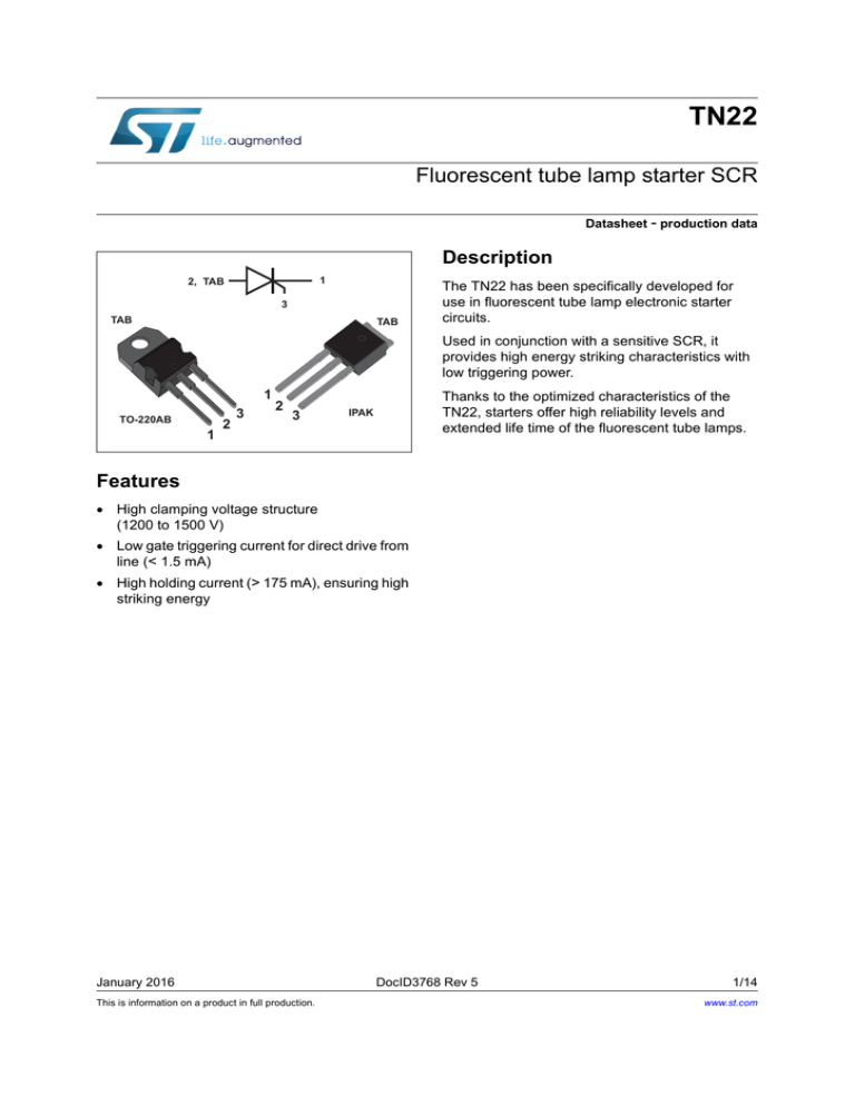
The TN22 has been specifically developed for
use in fluorescent tube lamp electronic starter
circuits.
Used in conjunction with a sensitive SCR, it
provides high energy striking characteristics with
low triggering power.
1
TO-220AB
1
2
3
2
3
Thanks to the optimized characteristics of the
TN22, starters offer high reliability levels and
extended life time of the fluorescent tube lamps.
IPAK
Features
High clamping voltage structure
(1200 to 1500 V)
Low gate triggering current for direct drive from
line (< 1.5 mA)
High holding current (> 175 mA), ensuring high
striking energy
January 2016
This is information on a product in full production.
DocID3768 Rev 5
1/14
www.st.com
Characteristics
1
TN22
Characteristics
Table 1. Absolute ratings (limiting values)
Symbol
Parameter
Value
Unit
VDRM
Repetitive peak off-state voltage
Tj = 110 °C
400
V
IT(RMS)
On-state RMS current
full sine wave (180° conduction angle)
Tc = 95 °C
2
A
IT(AV)
Mean on-state current
Full sinewave (180° conduction angle)
Tc = 95 °C
1.8
A
Non repetitive surge peak on-state current
(Tj initial = 25 °C)
tp = 8.3 ms
22
tp = 10 ms
20
I2t Value for fusing
tp = 10 ms
2
A2s
Critical rate of rise of on-state current
IG = 5 mA dIG/dt = 70 mA/µs
50
A/µs
Average gate power dissipation
300
mW
ITSM
I2t
dl/dt
PG(AV)
A
PGM
Peak gate power dissipation
tp = 20 µs
2
W
IGM
Peak gate current
tp = 20 µs
1
A
6
V
-40 to +150
-40 to +110
°C
260
°C
VRGM
Maximum peak reverse gate voltage
Tstg
Tj
Storage and operating junction temperature range
TL
Maximum lead temperature for soldering during 10 s at 4.5 mm
from case
Table 2. Electrical characteristics (Tj = 25 °C unless otherwise stated)
Symbol
Test conditions
Value
Unit
IGT
VD=12 V (DC), RL= 33
Max.
1.5
mA
VGT
VD=12 V (DC), RL= 33 RGK = 1 K
Max.
3
V
VGK = 0 V
Min.
175
mA
dV/dt
Linear slope up to VD = 67% VDRM, VGK = 0 V, Tj = 110 °C
Min.
500
V/µs
Min.
1200
VBR
ID = 5 mA, VGK = 0 V
Max.
1500
IH
V
Table 3. Static electrical characteristics (Tj = 25 °C unless otherwise stated)
Symbol
2/14
Test conditions
VTM
ITM = 2 A
IDRM
VDRM rated
tp = 380 µs
DocID3768 Rev 5
Value
Unit
Max.
3.1
V
Max.
0.1
mA
TN22
Characteristics
Table 4. Thermal resistance
Symbol
Parameter
Rth(j-a)
Junction to ambient
Rth(j-c)
Junction to case
IPAK
100
TO-220AB
60
Unit
°C/W
3
Figure 1. Maximum average power dissipation
versus average on-state current
(rectified sine wave)
Value
3:
Į
Figure 2. Average and DC on-state current
versus case temperature
(rectified sine wave)
Į Į
°C/W
,7$9 $
Į
Į
,7$9 $
7& &
Figure 3. Average on-state current versus
ambient temperature, free air convection
(rectified sine wave)
Figure 4. Variation of thermal impedance
junction to ambient versus pulse duration
,7$9 $
=WKMD&:
D
72$%
,3$.
72$%
'3$.,3$ .
7DPE &
WSV
(
DocID3768 Rev 5
(
(
(
(
(
(
3/14
14
Characteristics
TN22
Figure 5. Relative variation of gate trigger and
holding current versus junction temperature
,*7,+>7M@,*7,+>7M &@
,760$
W\SLFDOYDOXHV
Figure 6. Surge peak on-state current versus
number of cycles
,*7
WS PV
2QHF\FOH
,+
7M LQLWLDO &
7M&
1XPEHURIF\FOHV
Figure 7. Non-repetitive surge peak on-state
current for sinusoidal pulse
,760$,ðW$ðV
Figure 8. On-state characteristics
(maximum values)
,70$
7M LQLWLDO &
G,GW OLPLWDWLRQ
$V
,76 0
W S PV
,7506$
7& LQLWLDO &
72$%
7&
LDO &
&
& LQ LW LDO
7&
LQLWLDO &
&
& LQLWLDO
7& LQ LW LDO &
7& LQLWLDO &
7& LQ LW LDO &
,7506$
7M PD[ &WKHIDLOXUHPRGHZLOOEHVKRUWFLUFXLW
,3$.
Figure 10. Maximum allowable RMS current
versus time conduction and initial case
temperature
7M PD[ &WKHIDLOXUHPRGHZLOOEHVKRUWFLUFXLW
Figure 9. Maximum allowable RMS current
versus time conduction and initial case
temperature
7M PD[ 9WR 9
5' P
970 9
WSPV
7M &
7M &
WSV
WS V
4/14
DocID3768 Rev 5
TN22
Characteristics
Figure 11. Holding current versus gate-cathode resistance (typical values)
,+P$
7M &
5*.
DocID3768 Rev 5
5/14
14
Application information
TN22
2
Application information
2.1
Overview
The TN22 has been designed for use as a fluorescent tube starter switch.
As shown in Figure 12, the starter circuit is divided in five parts:
1.
Rectifier bridge: to rectify mains voltage.
2.
Voltage detector: RCD circuit used to switch on the TN22.
3.
Preheating time control: RC circuit used to switch on the SCR, so turn off the TN22.
4.
Ignition circuit: made of sensitive SCR and TN22 devices.
5.
Reset control: resistor used to discharge the C2 capacitor and to reset the circuit.
Figure 12. Electronic starter schematic
Starter circuit
SWITCH
IT
INDUCTANCE
BALLAST
R1
+
mains
FLUORESCENT
TUBE
D6
D2 – D5
4
TN22
Ignition circuit
mains
-
MAINS
VOLTAGE
SCR
1
+
C1
VS
2
6/14
D1
R4
+
Rectifier
3
R3
R2
Voltage detector
DocID3768 Rev 5
C2
5
Reset control
Preheating
time control
TN22
Application information
Three steps are necessary to ignite a fluorescent tube (see Figure 13):
preheating of the filament
ignition of the tube
“lighting” mode
Figure 13. The three operating steps of the electronic starter:
preheating, ignition and lighting
Preheating
IT (1 A/div)
Lighting
VS (500 V/div)
Ignition
2.2
Filament and tube preheating
The mains voltage is applied across the circuit and when it reaches a higher level than the
zener clamping voltage (VCL), a current flows through the resistor R1 and the capacitor C1.
The TN22 switches on when the voltage across its gate to cathode junction reaches the
triggering gate level (VGT).
As the TN22 is in on-state, a full sinusoidal current flows through the filaments (primary of
the rectifier bridge) that are warmed up. This current is limited by the input ballast. The TN22
remains on at each current zero crossing point because the gate is still powered by the C1
capacitor.
The preheating time duration is set with the RC circuit made of R3, R2 and C2, and
according to the voltage polarization fixed by the D1 drop voltage.
The preheating time is typically in the range of 2 to 3 seconds depending on the tube
characteristics.
DocID3768 Rev 5
7/14
14
Application information
2.3
TN22
Ignition step
When C2 is charged above the SCR triggering gate voltage (VGT), the SCR switches on.
The voltage across the TN22 gate to cathode junction is fixed to a negative value, which
allows a proper TN22 switch-off, with a high holding current (IH) level.
When the current reaches IH, the TN22 switches off and the ballast inductor generates a
high voltage pulse across the tube (see Figure 13). This over-voltage is clamped by the
TN22 to a value fixed by the breakdown voltage (VBR). A 1200 V to 1500 V level is
necessary to ensure a correct ignition of the fluorescent tubes.
Figure 14. Typical high voltage pulse of an electronic starter circuit
(P0130AA SCR, TN22)
VBR ≈ 1300 V
VS (200 V/div)
IH ≈ 225 mA
IT (50 mA/div)
If the lamp is not ignited after the first pulse, the starter circuit starts a new ignition
sequence. The pulse is regenerated until ignition of the tube lamp. If the lamp is not ignited
after several attempts, the starter circuit can automatically stop the ignition sequence.
Figure 15. Repetitive ignitions sequence
Pulse
IT (500 mA /div)
Mains voltage
f BURST= 50 Hz
2.4
V S (500 V/div)
Lighting state
When the lamp is ignited, the capacitor C2 is discharged through the resistors R2, R3 and
R4. The voltage across the lamp remains lower than the D6 clamping voltage (VCL),
avoiding the triggering of the TN22. The starter circuit remains in stand-by mode.
8/14
DocID3768 Rev 5
TN22
3
Package information
Package information
Epoxy meets UL94, V0
Lead-free packages
Recommended torque: 0.4 to 0.6 N·m
In order to meet environmental requirements, ST offers these devices in different grades of
ECOPACK® packages, depending on their level of environmental compliance. ECOPACK®
specifications, grade definitions and product status are available at: www.st.com.
ECOPACK® is an ST trademark.
3.1
IPAK package information
Figure 16. IPAK package outline
Note:
This package drawing may slightly differ from the physical package. However, all the
specified dimensions are guaranteed.
DocID3768 Rev 5
9/14
14
Package information
TN22
Table 5. IPAK package mechanical data
Dimensions
Ref.
Millimeters
Min.
Typ.
Max.
Min.
Typ.
Max.
A
2.20
2.40
0.086
0.094
A1
0.90
1.10
0.035
0.043
b
0.64
0.90
0.025
0.035
b2
b4
0.95
5.20
B5
5.43
0.037
0.204
0.30
0.213
0.012
c
0.45
0.60
0.017
0.023
c2
0.46
0.60
0.018
0.023
D
6
6.20
0.236
0.244
E
6.40
6.65
0.252
0.2618
e
e1
2.28
4.40
H
10/14
Inches
0.090
4.60
0.173
16.10
0.181
0.634
L
9
9.60
0.354
0.377
L1
0.8
1.20
0.031
0.047
L2
0.80
V1
10°
1.25
0.031
10°
DocID3768 Rev 5
0.049
TN22
3.2
Package information
TO-220AB package information
Figure 17. TO-220AB package outline
A
H2
Dia
C
L5
L7
L6
L2
F2
F1
D
L9
L4
F
M
G1
E
G
DocID3768 Rev 5
11/14
14
Package information
TN22
Table 6. TO-220AB package mechanical data
Dimensions
Ref.
Millimeters
Min.
Max.
Min.
Max.
A
4.40
4.60
0.17
0.18
b
0.61
0.88
0.024
0.035
b1
1.14
1.70
0.045
0.067
c
0.48
0.70
0.019
0.027
D
15.25
15.75
0.60
0.62
D1
12/14
Inches
1.27 typ.
0.05 typ.
E
10
10.40
0.39
0.41
e
2.40
2.70
0.094
0.106
e1
4.95
5.15
0.19
0.20
F
1.23
1.32
0.048
0.052
H1
6.20
6.60
0.24
0.26
J1
2.40
2.72
0.094
0.107
L
13
14
0.51
0.55
L1
3.50
3.93
0.137
0.154
L20
16.40 typ.
0.64 typ.
L30
28.90 typ.
1.13 typ.
P
3.75
3.85
0.147
0.151
Q
2.65
2.95
0.104
0.116
DocID3768 Rev 5
TN22
4
Ordering information
Ordering information
Figure 18. Ordering information scheme
71[
6WDUWOLJKWGHYLFH
2QVWDWH506FXUUHQW
$
7ULJJHULQJJDWHFXUUHQW0D[
P$
%UHDNGRZQYROWDJH
9
3DFNDJH
+ ,3$.
7 72$%
3DFNLQJ
%ODQN 7XEH
Table 7. Ordering information
Order code
5
Marking
Package
Weight
Base qty Delivery mode
TN22-1500H
TN22-1500
IPAK
0.4 g
75
Tube
TN22-1500T
TN22-1500
TO-220AB
2.0 g
50
Tube
Revision history
Table 8. Document revision history
Date
Revision
Oct-2000
1
First release.
17-Sep-2005
2
TO-220AB package added.
13-Aug-2009
3
Updated Figure 14. Added Figure 19 and Figure 20.
03-Jun-2014
4
Update IPAK package information and reformatted to
current standard.
5
Format updated to current standard.
Updated cover page.
Updated Figure 7, Figure 16 and Figure 18.
Updated Table 1 and Table 7.
18-Jan-2016
Changes
DocID3768 Rev 5
13/14
14
TN22
IMPORTANT NOTICE – PLEASE READ CAREFULLY
STMicroelectronics NV and its subsidiaries (“ST”) reserve the right to make changes, corrections, enhancements, modifications, and
improvements to ST products and/or to this document at any time without notice. Purchasers should obtain the latest relevant information on
ST products before placing orders. ST products are sold pursuant to ST’s terms and conditions of sale in place at the time of order
acknowledgement.
Purchasers are solely responsible for the choice, selection, and use of ST products and ST assumes no liability for application assistance or
the design of Purchasers’ products.
No license, express or implied, to any intellectual property right is granted by ST herein.
Resale of ST products with provisions different from the information set forth herein shall void any warranty granted by ST for such product.
ST and the ST logo are trademarks of ST. All other product or service names are the property of their respective owners.
Information in this document supersedes and replaces information previously supplied in any prior versions of this document.
© 2016 STMicroelectronics – All rights reserved
14/14
DocID3768 Rev 5


