XS
O
N3
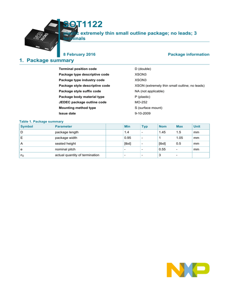
SOT1122
plastic extremely thin small outline package; no leads; 3
terminals
8 February 2016
Package information
1. Package summary
Terminal position code
D (double)
Package type descriptive code
XSON3
Package type industry code
XSON3
Package style descriptive code
XSON (extremely thin small outline; no leads)
Package style suffix code
NA (not applicable)
Package body material type
P (plastic)
JEDEC package outline code
MO-252
Mounting method type
S (surface mount)
Issue date
9-10-2009
Table 1. Package summary
Symbol
Parameter
Min
Typ
Nom
Max
Unit
D
package length
1.4
-
1.45
1.5
mm
E
package width
0.95
-
1
1.05
mm
A
seated height
[tbd]
-
[tbd]
0.5
mm
e
nominal pitch
-
-
0.55
-
mm
n2
actual quantity of termination
-
-
3
-
SOT1122
NXP Semiconductors
plastic extremely thin small outline package; no
leads; 3 terminals
2. Package outline
XSON3: plastic extremely thin small outline package; no leads; 3 terminals; body 1 x 1.45 x 0.5 mm
b
SOT1122
b1
1
4×
(2)
L1
3
L
e
2
e1
e1
4×
A
(2)
A1
D
type code
E
terminal 1
index area
pin 1 indication
0
1
Dimensions
Unit
mm
2 mm
scale
A(1)
max 0.50
nom
min
A1
b
b1
D
E
0.04
0.45
0.40
0.37
0.55
0.50
0.47
1.50
1.45
1.40
1.05
1.00
0.95
e
e1
L
0.35
0.55 0.425 0.30
0.27
L1
0.30
0.25
0.22
Notes
1. Dimension A is including plating thickness.
2. Can be visible in some manufacturing processes.
Outline
version
SOT1122
sot1122_po
References
IEC
JEDEC
JEITA
European
projection
Issue date
09-10-09
MO-252
Fig. 1. Package outline XSON3 (SOT1122)
SOT1122
Package information
All information provided in this document is subject to legal disclaimers.
8 February 2016
©
NXP Semiconductors N.V. 2016. All rights reserved
2/5
SOT1122
NXP Semiconductors
plastic extremely thin small outline package; no
leads; 3 terminals
3. Soldering
1.25
0.65
0.55
0.65 0.55
0.45
1.75
0.475
0.7
(2×)
0.6
(2×)
solder resist
solder paste = solderland
occupied area
Dimensions in mm
0.55
0.4
(2×)
0.3
(2×)
sot1122_fr
Fig. 2. Reflow soldering footprint for XSON3 (SOT1122)
SOT1122
Package information
All information provided in this document is subject to legal disclaimers.
8 February 2016
©
NXP Semiconductors N.V. 2016. All rights reserved
3/5
SOT1122
NXP Semiconductors
plastic extremely thin small outline package; no
leads; 3 terminals
4. Legal information
Disclaimers
Limited warranty and liability — Information in this document is believed
to be accurate and reliable. However, NXP Semiconductors does not give
any representations or warranties, expressed or implied, as to the accuracy
or completeness of such information and shall have no liability for the
consequences of use of such information. NXP Semiconductors takes no
responsibility for the content in this document if provided by an information
source outside of NXP Semiconductors.
In no event shall NXP Semiconductors be liable for any indirect, incidental,
punitive, special or consequential damages (including - without limitation lost profits, lost savings, business interruption, costs related to the removal
or replacement of any products or rework charges) whether or not such
damages are based on tort (including negligence), warranty, breach of
contract or any other legal theory.
Notwithstanding any damages that customer might incur for any reason
whatsoever, NXP Semiconductors’ aggregate and cumulative liability towards
customer for the products described herein shall be limited in accordance
with the Terms and conditions of commercial sale of NXP Semiconductors.
Right to make changes — NXP Semiconductors reserves the right to
make changes to information published in this document, including without
limitation specifications and product descriptions, at any time and without
notice. This document supersedes and replaces all information supplied prior
to the publication hereof.
SOT1122
Package information
All information provided in this document is subject to legal disclaimers.
8 February 2016
©
NXP Semiconductors N.V. 2016. All rights reserved
4/5
SOT1122
NXP Semiconductors
plastic extremely thin small outline package; no
leads; 3 terminals
5. Contents
1. Package summary........................................................ 1
2. Package outline............................................................ 2
3. Soldering....................................................................... 3
4. Legal information......................................................... 4
©
NXP Semiconductors N.V. 2016. All rights reserved
For more information, please visit: http://www.nxp.com
For sales office addresses, please send an email to: salesaddresses@nxp.com
Date of release: 8 February 2016
SOT1122
Package information
All information provided in this document is subject to legal disclaimers.
8 February 2016
©
NXP Semiconductors N.V. 2016. All rights reserved
5/5
