A PRACTICAL REVIEW OF
Common Mode and
Instrumentation Amplifiers
Addressed in
this tutorial are common mode voltage range
and common mode rejection as they pertain to instrumentation
amplifiers, their architectures, and their applications.
Eamon Nash, Analog Devices
I
nstrumentation amplifiers (in-amps)
amplify the difference between two signals. These differential signals typically
emanate from sensors such as resistive
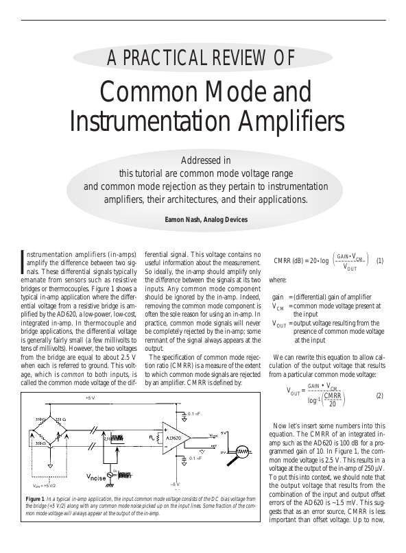
bridges or thermocouples. Figure 1 shows a
typical in-amp application where the differential voltage from a resistive bridge is amplified by the AD620, a low-power, low-cost,
integrated in-amp. In thermocouple and
bridge applications, the differential voltage
is generally fairly small (a few millivolts to
tens of millivolts). However, the two voltages
from the bridge are equal to about 2.5 V
when each is referred to ground. This voltage, which is common to both inputs, is
called the common mode voltage of the dif-
ferential signal. This voltage contains no
useful information about the measurement.
So ideally, the in-amp should amplify only
the difference between the signals at its two
inputs. Any common mode component
should be ignored by the in-amp. Indeed,
removing the common mode component is
often the sole reason for using an in-amp. In
practice, common mode signals will never
be completely rejected by the in-amp; some
remnant of the signal always appears at the
output.
The specification of common mode rejection ratio (CMRR) is a measure of the extent
to which common mode signals are rejected
by an amplifier. CMRR is defined by:
1
GAIN• VCM
CMRR (dB) = 20 • log ––––––––––
VOUT
(1)
gain = (differential) gain of amplifier
VCM = common mode voltage present at
the input
VOUT = output voltage resulting from the
presence of common mode voltage
at the input
We can rewrite this equation to allow calculation of the output voltage that results
from a particular common mode voltage:
GAIN • VCM
VOUT = –––––––––––
CMRR
log–1 ––––––
20
1
+5 V
2
where:
2
(2)
0.1 µF
0.1 µF
0v
Vcm = +5 V/2
–5 V
Figure 1. In a typical in-amp application, the input common mode voltage consists of the DC bias voltage from
the bridge (+5 V/2) along with any common mode noise picked up on the input lines. Some fraction of the common mode voltage will always appear at the output of the in-amp.
Now let’s insert some numbers into this
equation. The CMRR of an integrated inamp such as the AD620 is 100 dB for a programmed gain of 10. In Figure 1, the common mode voltage is 2.5 V. This results in a
voltage at the output of the in-amp of 250 µV.
To put this into context, we should note that
the output voltage that results from the
combination of the input and output offset
errors of the AD620 is ~1.5 mV. This suggests that as an error source, CMRR is less
important than offset voltage. Up to now,
however, we have been talking only about
common mode rejection of DC signals.
AC and DC Common Mode Rejection
As shown in Figure 1, common mode signals can be steady-state DC voltages (such
as the 2.5 V from the bridge) or they can be
AC signals such as external interference. In
industrial applications, the most common
cause of external interference is pickup
from 50/60 Hz mains sources (e.g., lights,
motors, or any equipment running on the
mains). In differential measurement applications, interference tends to be induced
equally onto both in-amp inputs. The interfering signal therefore appears as a common
mode signal to the in-amp. This signal will
be superimposed on the DC common
mode input voltage (from the bridge). At
the output of the in-amp, we will see an
attenuated version of the overall input common mode signal.
While a DC offset can be easily removed
by trimming or calibration, AC errors
appearing at the output are much more
troublesome. If, for example, the input circuit picks up 50 Hz or 60 Hz interference
from the mains, the AC voltage that appears
at the output will reduce the resolution of
the application. Filtering out this interference can be expensive and is feasible only
in very slow applications. Obviously, high
common mode rejection over frequency
will help minimize the effects of external
common mode interference.
We can conclude that specifying CMRR
over frequency is in practice more important than specifying it at DC. Data sheets
for integrated in-amps should ideally list the
CMRR at 50/60 Hz on the specifications
page and include a plot of CMRR vs. frequency in the plots section of the data sheet.
Figure 2 shows the change in CMRR over
frequency for the AD623, a low-cost integrated in-amp. The CMRR remains flat up
to 100 Hz and then begins to decrease. In
this example, interference from 50/60 Hz
mains interference will be well suppressed
by the AD623. However, we also need to be
conscious of interference caused by harmonics of the mains frequency. In industrial environments, harmonics of the mains
frequency can be significant up to the seventh harmonic (350/420 Hz). In the case of
the AD623, we see that the CMRR has
dropped to ~90 dB at a gain of 10 at these
frequencies. This results in a common
mode gain of –70 dB, still enough to suppress most common mode interference.
age that results from the presence of DC
common mode voltage is given by:
VOUT = Vcm
R2R4
1 1– –––––
2
R1R3
(4)
Using Equation 1, the formula for the
CMRR of the circuit comes out to be:
CMRR = 20•log
Figure 2. The CMRR of the AD623, when used
as a single-supply in-amp, is flat out to ~100 Hz
but begins to degrade thereafter. As the programmed gain is increased, CMRR also increases.
We will now look at different in-amp
architectures. It will become clear that
choice of architecture and the precision of
passive components affects both the AC and
DC CMRR.
The 2 Op-Amp In-Amp
Figure 3 is a circuit diagram for a basic 2
op-amp in-amp. The differential gain is
given by [1]:
VOUT = (VIN+ – VIN– )
R1
1 1+ –––
2
R2
(3)
where:
R1 = R4 and R2 = R3
With R1 equal to 10 kΩ, and R2 equal to
1 kΩ, the differential gain is equal to 11.
We can see from Equation 3 that a programmed gain of 1 is fundamentally not
achievable.
Common Mode Gain. The output volt-
A2
A1
Figure 3. The input common mode range of a 2 opamp in-amp decreases with decreasing gain (a gain
of unity is not achievable). Resistor mismatch sets
the CMRR at DC, while higher frequency CMRR is
determined by the phase shift of Vin+ through A1.
1
GAIN
––––––––
R2R4
1– ––––
R1R3
2
(5)
Because the resistor ratio in the denominator is always close to 1, regardless of the
in-amp’s gain, we can conclude that the
CMRR or a 2 op-amp in-amp increases with
gain.
It is common to specify the accuracy of
resistor networks in terms of resistor-to-resistor percentage mismatch. We can rewrite
Equation 5 to reflect this:
CMRR = 20•log
GAIN 100
1––––––––––
%MISMATCH 2
•
(6)
Any mismatch between the four gain setting resistors will have a direct impact on
the CMRR. Precision resistor networks are
typically trimmed for maximum accuracy at
ambient temperature. Any mismatch in the
temperature drift of the resistors will further
degrade the CMRR. Clearly, the key to high
common mode rejection is a network of
resistors that are well matched from the perspective of both resistive ratio and relative
drift. It should be noted that the absolute
values of the resistors and their absolute
drifts are of no consequence. Matching is
the key.
Integrated instrumentation amplifiers are
particularly well suited to meeting the combined needs of ratio matching and temperature tracking of the gain-setting resistors.
While thin film resistors fabricated on silicon have an initial tolerance of up to ±20%,
laser trimming during production allows the
ratio error between the resistors to be cost
effectively reduced to 0.01% (100 ppm).
Furthermore, the tracking between the temperature coefficients of the thin film resistors is inherently low and is typically
<3 ppm/ºC (0.0003%/ºC).
The plot in Figure 4A exhibits the practical
results, at ambient temperature, of resistor
mismatch. The CMRR of the circuit in
Figure 3 (gain = 11) was measured using four
resistors that had a mismatch of almost exactly
0.1% (R1 = 9999.5 Ω, R2 = 999.76 Ω, R3 =
1000.2 Ω, R4 = 9997.7 Ω). As expected, the
(A)
(B)
INPUT
50mV/div
OUTPUT
0.5mV/div
1ms/div
Figure 4. A mismatch of 0.1% between the four
gain-setting resistors will determine the low-frequency CMRR of a 2 op-amp in-amp. The difference between the closed loop gains of the two opamps will cause degradation in the CMRR over frequency. A 200 mV mains harmonic at 180 Hz will
produce 800 µV at the in-amp’s output.
CMRR at DC was measured at ~84 dB (the
theoretical value is 85 dB). As the frequency
increases, however, the CMRR quickly
degrades. Figure 4B is an oscilloscope photo
of the output voltage that results from mains
interference. A 200 mV peak-to-peak harmonic of the mains frequency at 180 Hz
results in an output voltage of ~800 µV. To
put this into context, a 12-bit data acquisition system with an input range of 0 V to
2.5 V has a least significant bit (LSB)
weighting of 610 µV.
The degradation in CMRR over frequency is caused by the phase shift of the
VIN+ signal through A1. This sets up a vector error between VIN. and the output of A1.
For infinite CMRR, these signals would
have to have identical phase and amplitude
from a common mode perspective. This
would only be possible if there were no
delay thorugh A1. Choosing a well-matched
high-speed dual op-amp will extend the frequency over which the CMRR stays flat, but
high-speed op-amps also have a tendency to
pick up high-frequency external interference. An alternative solution to this problem is to use an AC trim capacitor between
the inverting input of A1 and ground [1].
This trim, however, would need to be done
by hand for every in-amp produced.
So the plot of CMRR vs. frequency in
Figure 4 is influenced by two distinct
parameters. The CMRR at low frequencies
is related directly to the mismatch between
the gain-setting resistors, while the degradation in CMRR at higher frequencies is
caused by the different closed loop gains of
the op-amps.
Common Mode Range. The input common mode range of the 2 op-amp in-amp is
affected by the programmed gain. In Figure
3, we can see that A1 is operating at a closed
loop gain of 1.1. Any common mode voltage
present at the input will be amplified by this
amount by A1 (i.e., 1.1 3 the common
mode voltage appears at the output of A1).
Now consider a case where the in-amp has
a programmed gain of 1.1 (R1 = 1 kΩ, R2 =
10 kΩ, R3 = 10 kΩ, R4 = 1 kΩ). Now A1 is
operating at a closed loop gain of 11.
Because the common mode voltage is being
amplified by A1, the input common mode
range is severely restricted by the output
swing of A1. The problem is especially
acute in applications where low voltage supplies are mandatory, The use of rail-to-rail
amplifiers will improve matters somewhat
by adding some more headroom.
The 3 Op-Amp In-Amp
The 3 op-amp in-amp architecture (see
Figure 5) is a popular choice for both discrete and integrated in-amps. The overall
gain transfer function is quite complicated,
but if R1 = R2 = R3 = R4, the transfer function simplifies to [1]:
1
R5 + R6
VOUT = (VIN+ – VIN– ) 1+ –––––––
RG
2
(7)
R5 and R6 are typically set to the same
value, usually somewhere between 10 kΩ
and 50 kΩ. The circuit’s overall gain can be
adjusted from unity to an arbitrarily high
value simply by changing the value of RG.
Common Mode Gain. As we would
expect, the common mode gain of the inamp should ideally be equal to zero. To
work out the common mode gain, let’s
imagine that there is only a common mode
voltage of Vcm present at the inputs (i.e.,
Vin+ = Vin– = Vcm). As there is no voltage
drop across RG, the voltage on the outputs
of each of the amplifiers, A1 and A2, is also
equal to Vcm. So to a first approximation
(i.e., assuming A1 and A2 are ideally
10 kΩ
10 kΩ
10 kΩ
10 kΩ
10 kΩ
10 kΩ
Figure 5. In a 3 op-amp in-amp, a mismatch of
0.1% among resistors R1, R2, R3, and R4 will
result in a worst case CMRR (at a gain of 1) of
60 dB. Drift mismatch between resistors will further reduce the CMRR. Monolithic in-amps
offer greater accuracy at lower cost.
matched) the common mode gain of the
first stage is equal to unity and is independent of the programmed gain.
Assuming that op-amp A3 is ideal, the
common mode gain of the second stage is
given by:
1
VOUT R2 + R1
R4
R2
–––– = ––––––– • ––––––– – ––
VCM
R1
R3 + R4 R1
2
(8)
Plugging this into Equation 1, the equation for the common mode rejection ratio
becomes:
CMRR = 20•log
1
GAIN
2
––––––––––––––––––
R2+R1 R4
R2 (9)
–––––––– • –––––––– – ––
R1 R3+R4 R1
The denominator of this equation is more
complicated than it is for the 2 op-amp inamp. Just as in Equation 6, however, the
denominator can be replaced by the percentage mismatch between the resistors:
CMRR = 20 • log
GAIN•100
1 %–––––––––
2
MISMATCH
(10)
Now, if all four resistors in Equation 9 are
equal (or even if R1 = R3 and R2 = R4), the
denominator will reduce to zero. But any
mismatch between the four resistors will
cause a portion of the common mode voltage to appear at the output. Similar to the
case of the 2 op-amp in-amp, any mismatch
between the temperature drift of the resistors will further degrade the CMRR as the
temperature changes.
AC CMRR. If A1 and A2 are well
matched (i.e., have similar closed loop
bandwidths), the CMRR will not tend to
degrade so quickly as it does with the 2 opamp in-amp. Again referring to Figures 2
and 4, we see that the CMRR of the 3 opamp in-amp remains relatively flat out to
A1
A3
As the industry moves to lower supply voltages, this issue becomes more critical with
less and less headroom being available. As
in the case of the 2 op-amp in-amp, the use
of rail-to-rail op-amps maximizes available
headroom. A rail-to-rail output stage (A3) is
of little use, though, if the output voltages of
the input stage, A1 and A2, are being
clipped because of excessive input voltage,
common mode voltage, or gain.
µF
µF
A2
Figure 6. The AD623 in-amp follows the architecture of a classic 3 op-amp in-amp. By shifting both
input voltages upward by 0.6 V, single-supply
operation is possible even in the presence of very
low or slightly negative common mode voltages.
100 Hz while the CMRR of a 2 op-amp inamp begins to degrade at ~10 Hz.
Common Mode Range. As we have previously noted, the common mode gain of the
first stage of a 3 op-amp in-amp is unity,
with the result that the common mode voltage appears at the output of A1 and A2 in
Figure 5. The differential input voltage,
V DIFF, however, appears across the gain
resistor. The resulting current that must
flow through R5 and R6 means that the
voltage on A1 will rise above Vcm and the
voltage on A2 will drop below Vcm as the
differential input voltage increases. Therefore, as the gain and/or input signal increases, so does this “spreading” of the voltages on A1 and A2, ultimately to be limited
by the supply rails.
We can conclude that the achievable
ranges on the common mode voltage, the
differential input voltage, and the gain are
interrelated. For example, increasing the
gain reduces both common mode range and
input voltage range. By the same token,
increasing the common mode voltage tends
to limit the differential input range and the
maximum achievable gain. If the output
swings of the input stage op-amps are
known, the relationship governing input
range, common mode range, and gain can
be well defined for a particular 3 op-amp inamp [2].
Single-Supply In-Amp for
Low Common Mode Applications
The AD623, a low-cost single-supply railto-rail in-amp (see Figure 6), follows the
classic 3 op-amp in-amp architecture. But
before being applied to the input stage opamps, both the inverting and noninverting
input voltages are shifted upward by 0.6 V
(i.e., a diode drop) as they each pass
through a pnp transistor.
To understand the consequences of this
level shifting, we should consider the conditions under which the in-amp is usually
operated. In Figure 7, it is shown amplifying
the signal from a J-type thermocouple. The
in-amp, along with the A/D converter into
which it feeds, is powered by a single supply
of +5 V. The temperature to be measured
ranges from –200ºC to 200ºC, which corresponds to a thermocouple voltage of –7.890
mV to +10.777 mV.
As is normal practice, one side of the thermocouple is grounded to allow the necessary
bias currents to flow into the in-amp. As a
result, the common mode voltage, which is
halfway between the inverting and noninverting input voltages, is very close to
ground. Indeed, as the voltage from the thermocouple becomes negative, the effective
common mode voltage also goes negative.
In a conventional 3 op-amp in-amp, the
voltage-spreading effect of the input stage
would cause the output voltage on one of
the input op-amps to run into the ground
rail as soon the thermocouple voltage gets
above 0 V. The level shifting architecture in
Figure 6 gets around this problem by effectively adding 0.6 V to the common mode
voltage. This creates more headroom to
ground and allows the output voltages of A1
and A2, which are rail-to-rail, to stay in a
Reprinted from Sensors, July 1998
www.sensorsmag.com
Copyright© 1998 by Helmers Publishing, Inc.
174 Concord St., Peterborough, NH 03458
All Rights Reserved
Figure 7. The input stage level shifting of the
AD623 is ideally suited to low common mode
applications where only a single supply is available. Over a –200ºC to 200ºC temperature range,
the J-type thermocouple delivers a voltage ranging
from –7.890 mV to 10.777 mV. A gain of 91.9
maps this voltage into the 1–3 V range (i.e., 2 V
±1 V) of the single-supply AD7776 A/D converter.
linear region, even when the input voltage
and the common mode voltage go below
ground. The input voltage can go negative
by as much as 150 mV, depending on the
programmed gain and the common mode
voltage [2].
In this example, the programmed gain on
the in-amp is 91.9 (RG =1.1 kΩ). The voltage on the in-amp’s REF pin has been set to
2 V. So as the thermocouple voltage varies
from –7.890 mV to +10.777 mV, the inamp’s output voltage ranges from 1.274 V to
2.990 V (relative to ground). This voltage
swing fits comfortably into the input range
of the A/D converter, which is 2 V ±1 V. ■
References
1. Charles Kitchin and Lew Counts. Aug.
1991. Instrumentation Amplifier Applications
Guide, Analog Devices:6-10. Available at
www.analog. com/AD623/
2. AD623 Single Supply, Rail-to-Rail, Low Cost
Instrumentation Amplifier. Oct. 1997. Analog
Devices:15. Available at http://www.analog.
com/AD623/
Eamon Nash is an Applications Engineer at
Analog Devices’ Advanced Linear Products
Group, Analog Devices, 804 Woburn St.,
Wilmington, MA 01887; 781-937-1239, fax
781-937-1024, eamon.nash@analog.com


