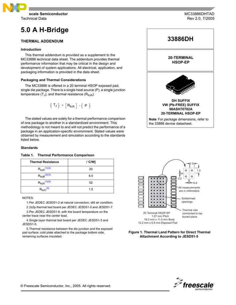
MC33886DHTAD
Rev 2.0, 7/2005
Freescale Semiconductor
Technical Data
5.0 A H-Bridge
33886DH
THERMAL ADDENDUM
Introduction
This thermal addendum is provided as a supplement to the
MC33886 technical data sheet. The addendum provides thermal
performance information that may be critical in the design and
development of system applications. All electrical, application, and
packaging information is provided in the data sheet.
20-TERMINAL
HSOP-EP
Packaging and Thermal Considerations
The MC33886 is offered in a 20 terminal HSOP exposed pad,
single die package. There is a single heat source (P), a single junction
temperature (TJ), and thermal resistance (RθJA).
TJ
=
RθJA
.
DH SUFFIX
VW (Pb-FREE) SUFFIX
98ASH70702A
20-TERMINAL HSOP-EP
P
The stated values are solely for a thermal performance comparison
of one package to another in a standardized environment. This
methodology is not meant to and will not predict the performance of a
package in an application-specific environment. Stated values were
obtained by measurement and simulation according to the standards
listed below.
Note For package dimensions, refer to
the 33886 device datasheet.
Standards
Table 1.
Thermal Performance Comparison
Thermal Resistance
[°C/W]
(1)(2)
RθJA
20
RθJB(2)(3)
6.0
RθJA(1)(4)
52
RθJC
(5)
1.0
1.0
0.2
1.0
0.2
* All measurements
are in millimeters
NOTES:
Soldermast
openings
1.Per JEDEC JESD51-2 at natural convection, still air condition.
2.2s2p thermal test board per JEDEC JESD51-5 and JESD51-7.
3.Per JEDEC JESD51-8, with the board temperature on the
center trace near the center lead.
4.Single layer thermal test board per JEDEC JESD51-3 and
JESD51-5.
5.Thermal resistance between the die junction and the exposed
pad surface; cold plate attached to the package bottom side,
remaining surfaces insulated.
© Freescale Semiconductor, Inc., 2005. All rights reserved.
20 Terminal HSOP-EP
1.27 mm Pitch
16.0 mm x 11.0 mm Body
12.2 mm x 6.9 mm Exposed Pad
Thermal vias
connected to top
buried plane
Figure 1. Thermal Land Pattern for Direct Thermal
Attachment According to JESD51-5
A
AGND
FS
IN1
V+
V+
OUT1
OUT1
DNC
PGND
PGND
20
19
18
17
16
15
14
13
12
11
1
2
3
4
5
6
7
8
9
10
DNC
IN2
D1
CCP
V+
OUT2
OUT2
D2
PGND
PGND
33886 Terminal Connections
20-Terminal HSOP
1.27 mm Pitch
16.0 mm x 11.0 mm Body
12.2 mm x 6.9 mm Exposed Pad
Figure 2. Thermal Test Board
Device on Thermal Test Board
Material:
Outline:
Single layer printed circuit board
FR4, 1.6 mm thickness
Cu traces, 0.07 mm thickness
80 mm x 100 mm board area,
including edge connector for thermal
testing
Area A:
Cu heat-spreading areas on board
surface
Ambient Conditions:
Natural convection, still air
Table 2.
Thermal Resistance Performance
Thermal
Resistance
Area A (mm2)
°C/W
RθJA
0.0
52
300
36
600
32
0.0
10
300
7.0
600
6.0
RθJS
RθJA is the thermal resistance between die junction and
ambient air.
RθJS is the thermal resistance between die junction and the
reference location on the board surface near a center lead of the
package (see Figure 2).
33886DH
2
Analog Integrated Circuit Device Data
Freescale Semiconductor
Thermal Resistance [ºC/W]
60
50
40
30
x
RθJA
20
10
0
0
300
Heat spreading area A [mm²]
600
Figure 3. Device on Thermal Test Board RθJA
Thermal Resistance [ºC/W]
100
x
RθJA
10
1
0.1
1.00E-03
1.00E-02 1.00E-01 1.00E+00 1.00E+01 1.00E+02 1.00E+03 1.00E+04
time[s]
Time(s)
Figure 4. Transient Thermal Resistance RθJA
Device on Thermal Test Board Area A = 600 (mm2)
33886DH
Analog Integrated Circuit Device Data
Freescale Semiconductor
3
How to Reach Us:
Home Page:
www.freescale.com
E-mail:
support@freescale.com
USA/Europe or Locations Not Listed:
Freescale Semiconductor
Technical Information Center, CH370
1300 N. Alma School Road
Chandler, Arizona 85224
+1-800-521-6274 or +1-480-768-2130
support@freescale.com
Europe, Middle East, and Africa:
Freescale Halbleiter Deutschland GmbH
Technical Information Center
Schatzbogen 7
81829 Muenchen, Germany
+44 1296 380 456 (English)
+46 8 52200080 (English)
+49 89 92103 559 (German)
+33 1 69 35 48 48 (French)
support@freescale.com
Japan:
Freescale Semiconductor Japan Ltd.
Headquarters
ARCO Tower 15F
1-8-1, Shimo-Meguro, Meguro-ku,
Tokyo 153-0064
Japan
0120 191014 or +81 3 5437 9125
support.japan@freescale.com
Asia/Pacific:
Freescale Semiconductor Hong Kong Ltd.
Technical Information Center
2 Dai King Street
Tai Po Industrial Estate
Tai Po, N.T., Hong Kong
+800 2666 8080
support.asia@freescale.com
For Literature Requests Only:
Freescale Semiconductor Literature Distribution Center
P.O. Box 5405
Denver, Colorado 80217
1-800-441-2447 or 303-675-2140
Fax: 303-675-2150
LDCForFreescaleSemiconductor@hibbertgroup.com
MC33886DHTAD
Rev 2.0
7/2005
Information in this document is provided solely to enable system and software
implementers to use Freescale Semiconductor products. There are no express or
implied copyright licenses granted hereunder to design or fabricate any integrated
circuits or integrated circuits based on the information in this document.
Freescale Semiconductor reserves the right to make changes without further notice to
any products herein. Freescale Semiconductor makes no warranty, representation or
guarantee regarding the suitability of its products for any particular purpose, nor does
Freescale Semiconductor assume any liability arising out of the application or use of any
product or circuit, and specifically disclaims any and all liability, including without
limitation consequential or incidental damages. “Typical” parameters that may be
provided in Freescale Semiconductor data sheets and/or specifications can and do vary
in different applications and actual performance may vary over time. All operating
parameters, including “Typicals”, must be validated for each customer application by
customer’s technical experts. Freescale Semiconductor does not convey any license
under its patent rights nor the rights of others. Freescale Semiconductor products are
not designed, intended, or authorized for use as components in systems intended for
surgical implant into the body, or other applications intended to support or sustain life,
or for any other application in which the failure of the Freescale Semiconductor product
could create a situation where personal injury or death may occur. Should a Buyer
purchase or use Freescale Semiconductor products for any such unintended or
unauthorized application, the Buyer shall indemnify and hold Freescale Semiconductor
and its officers, employees, subsidiaries, affiliates, and distributors harmless against all
claims, costs, damages, and expenses, and reasonable attorney fees arising out of,
directly or indirectly, any claim of personal injury or death associated with such
unintended or unauthorized use, even if such claim alleges that Freescale
Semiconductor was negligent regarding the design or manufacture of the part.
Freescale™ and the Freescale logo are trademarks of Freescale Semiconductor, Inc.
All other product or service names are the property of their respective owners.
© Freescale Semiconductor, Inc., 2005. All rights reserved.
