Battery Management System Tutorial
Today’s electronic devices have higher mobility and are greener than ever before. Battery advancements are
fueling this progression in a wide range of products from portable power tools to plug-in hybrid electric
vehicles and wireless speakers. In recent years, the efficiency of a battery in terms of how much power it can
output with respect to size and weight has dramatically improved. Think about how heavy and bulky a car
battery is. Its main purpose is to start the car. With recent advancements, you can purchase a lithium-ion
battery to jump start your car, and it only weighs a couple pounds and is the size of your hand.
The ongoing transformation of battery technology has prompted many newcomers to learn about designing
battery management systems. This article provides a beginner’s guide to the battery management system
(BMS) architecture, discusses the major functional blocks, and explains the importance of each block to the
battery management system.
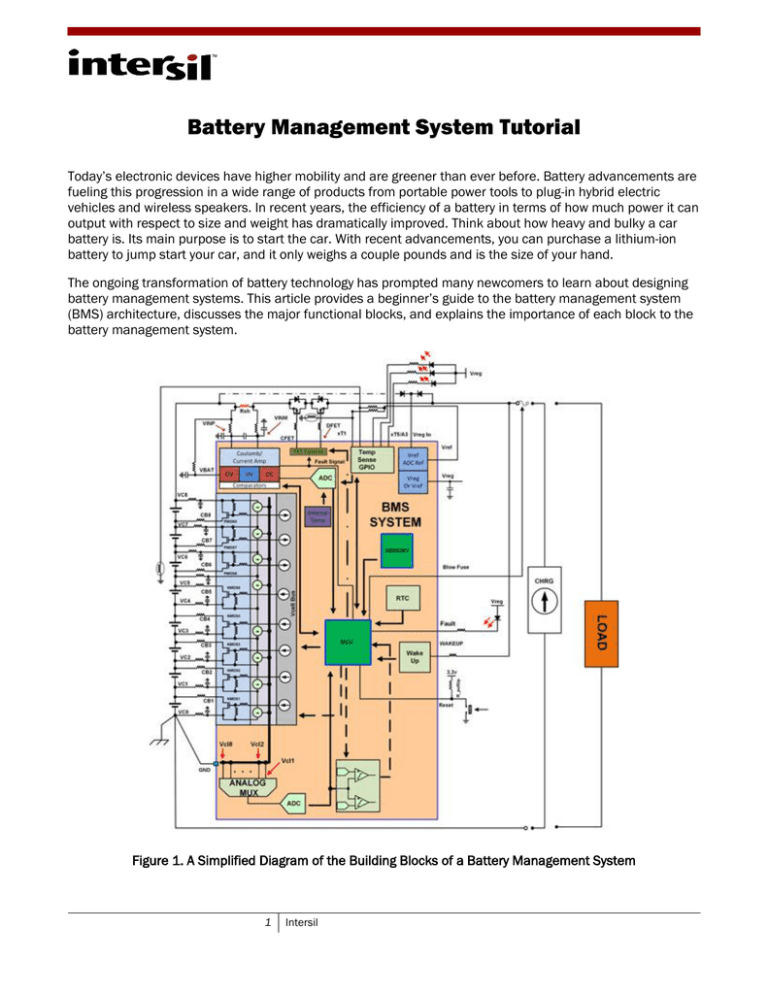
Figure 1. A Simplified Diagram of the Building Blocks of a Battery Management System
1
Intersil
Building Blocks of a Battery Management System
A battery management system can be comprised of many functional blocks including: cutoff FETs, a fuel
gauge monitor, cell voltage monitor, cell voltage balance, real time clock (RTC), temperature monitors and a
state machine. There are many types of battery management ICs available. The grouping of the functional
blocks varies widely from a simple analog front end that offers balancing and monitoring and requires a
microcontroller (MCU), to a standalone, highly integrated solution that runs autonomously. Now let’s take a
look at the purpose and the technology behind each block, as well as the pros and cons of the technology.
Cutoff FETs and FET Driver
A FET driver functional block is responsible for the connection and isolation of the battery pack between the
load and charger. The behavior of the FET driver is predicated on measurements from battery cell voltages,
current measurements and real-time detection circuitry. Figures 2A and 2B illustrate two different types of
FET connections between the load and charger, and the battery pack.
Figure 2. Cutoff FET Schematic Illustrations for (A) Single Connection for the Load and Charger; (B) Two
Terminal Connection that Allows for Charging and Discharging Simultaneously
Figure 2A requires the least amount of connections to the battery pack and limits the battery pack operating
modes to charge, discharge or sleep. The current flow direction and the behavior of a specific real-time test
determines device’s state. For example, Intersil’s ISL94203 standalone battery pack monitor has a CHMON
input that monitors the voltage on the right side of the cutoff FETs. If a charger is connected and the battery
pack is isolated from the charger, the current injected towards the battery pack will cause the voltage to rise
to the charger’s maximum supply voltage. The voltage level at CHMON is tripped letting the BMS device
know a charger is present. A load connection is determined by injecting a current into the load to determine
if a load is present. If the voltage at the pin does not raise significantly when current is injected, the outcome
determines a load is present. The FET driver’s DFET is then turned on. The connection scheme for Figure 2B
allows the battery pack to operate while charging.
FET drivers can be designed to connect to the high-side or low-side of a battery pack. A high-side connection
requires a charge pump driver to activate the NMOS FETs. Using a high-side driver allows for a solid ground
reference for the rest of the circuitry. Low-side FET driver connections are found in some integrated solutions
2
Intersil
to reduce cost because a charge pump is not needed. A low-side connection does not require high voltage
devices, which consume a larger die area. Using the cutoff FETs on the low-side floats the battery pack’s
ground connection, making it more susceptible to noise injected into the measurement, which can affect the
performance of some ICs.
Fuel Gauge / Current Measurements
The fuel gauge functional block keeps track of the charge entering and exiting the battery pack. Charge is
the product of current and time. There are several different techniques that can be used when designing a
fuel gauge. A current sense amplifier and an MCU with an integrated low resolution ADC is one method of
measuring the current. The current sense amplifier operates in high common-mode environments and
amplifies the signal, enabling higher resolution measurements. This design technique sacrifices dynamic
range. Other techniques are to use a high resolution ADC, or to purchase a costly fuel gauge IC.
Understanding the behavior of the load in terms of current consumption versus time determines the best
type of fuel gauge design.
The most accurate and cost efficient solution is to measure the voltage across a sense resistor using a 16bit or higher ADC with low offset and high common-mode rating. A high resolution ADC offers a large dynamic
range at the expense of speed. If the battery is connected to an erratic load such as an electric vehicle, the
slow ADC may miss high magnitude and high frequency current spikes that are delivered to the load. For
erratic loads, a SAR ADC with perhaps a current sense amplifier front end may be more desirable. Any offset
error results in an overall error in the amount of charge in the battery. Measurement errors over time will
cause significant battery pack charge status errors. A measurement offset of 50µV or less with 16-bit
resolution is adequate in measuring charge.
With most current measurement blocks, there are analog comparators monitoring for short circuit and over
current conditions. The analog comparator signal is directly connected to FET drivers to minimize latency
between the event and isolating the battery pack from the load or charger. A latency time of several 10s of
microseconds is adequate for most applications, and in most applications, the faster the time to disconnect
the battery, the better.
Cell Voltage and Maximizing Battery Lifetime
Monitoring the cell voltage of each cell within a battery pack is essential in determining its overall health. All
cells have an operating voltage window that charging and discharging should occur to ensure proper
operation and battery life. If an application is using a battery with a lithium chemistry, the operating voltage
typically ranges between 2.5V and 4.2V. The voltage range is chemistry dependent. Operating the battery
outside the voltage range significantly reduces the lifetime of the cell and can render the cell useless.
Cells are connected in series and parallel to form a battery pack. A parallel connection increases the current
drive of the battery pack, while a series connection increases the overall voltage. Cell voltages are like
everything that is manufactured. A cell’s performance has a distribution: at time equal zero, the cells charge
and discharge rates within a battery pack are the same. As each cell is cycled between charge and
discharge, the rate at which each cell charges and discharges changes, resulting in a spread distribution
across a battery pack. A simplistic means of determining if a battery pack is charged is to monitor each cell’s
voltage to a set voltage level. The first cell voltage to reach the voltage limit trips the battery pack charged
limit. If the battery pack had a weaker than average cell, this would result in the weakest cell reaching the
limit first and the rest of the cells not fully charged. A charging scheme as described does not maximize the
battery pack ON time per charge. The charging scheme also reduces the lifetime of the battery pack because
more charge and discharge cycles are needed. A weaker cell discharges faster. The same type of occurrence
happens on the discharge cycle. The weaker cell trips the discharge limit first leaving the rest of the cells
with charge remaining.
3
Intersil
Figure 3. Different Types of Cell Balancing (A) Bypass Cell Balancing FETs are Used to Slow the Charge Rate
of a Cell During the Charge Cycle; (B) Active Balancing is Used During the Discharge Cycle to Steal Charge
from a Strong Cell and Give the Charge to a Weak Cell
There are two means of improving the ON time of a battery pack per charge. The first one is slowing the
charge to the weakest cell receives during the charge cycle. This is achieved by connecting a bypass FET
with a current limiting resistor across the cell (see Figure 3A). This takes the current from the cell with the
highest current resulting in a slowing of charge to the cell, allowing the other cells in the battery pack to
catch up. The ultimate goal is to maximize the battery pack’s charge capacity, which is achieved by having all
the cells reach the fully charged limit simultaneously.
The battery pack can be balanced on the discharge cycle by implementing a charge displacement scheme. A
charge displacement scheme is achieved by taking charge via inductive coupling or capacitive storage from
the alpha cell and injecting the stored charge into the weakest cell. This slows the time it takes weakest cell
to reach the discharge limit. This is known as active balancing (see Figure 3B).
Battery packs with one to four batteries in parallel and three or more in series benefit the most from
balancing. As the parallel combinations increase per cell, the weak cell’s performance is averaged with other
cells in parallel. The performance distribution between cells is tighter. The benefit of having more cells in
parallel is also a detriment because it is harder to find the weaker cell in a battery pack. A battery pack
sitting idle could be burning charge due to the strong cells propping up the weaker cell.
The cell voltage and balancing circuitry receives the harshest treatment from hot plug events. There is not an
OFF button on a battery. Connecting the circuity to a battery, load or charger can result in large transients
occurring at the inputs of the device. A designer should be aware of the maximum rating of sensitive pins.
The maximum voltage rating of a pin is a key specification to determining the likelihood that a transient
event will damage the circuitry. The rule of thumb is the higher the voltage rating of a pin, the more robust
the part will be in suppressing transients.
An IC manufacturer designing with a high voltage process ensures that the device is protected from transient
events at the expense of design with large geometries. This raises the cost of the device. Other IC
manufactures will design with a low voltage process and stack the devices such that a device never exceeds
4
Intersil
the process rating. This approach relies upon circuitry such as capacitors, resistors and diodes to suppress
the transient before it reaches the pin. Both manufacturing types require the use of diodes, resistors and
capacitors to dampen transients. Using a high voltage rated IC adds further protection against harmful and
extraneous signals. Both design approaches will work but the lower voltage rated device may require more
tweaking in the development stage to ensure protection against harmful events.
The acquisition time of a voltage cell measurement is dependent on the load behavior as well as the number
of cells to scan. Erratic behaving loads require fast scan times to monitor a cell’s out of bounds condition. A
SAR ADC is often used to achieve quick measurements in a short period of time. A SAR ADC consumes more
power and has less resolution.
Temperature Monitoring
Today’s batteries deliver a lot of current while maintaining a constant voltage, which can lead to a runaway
condition that causes the battery to catch fire. The chemicals used to construct a battery are highly volatile,
and a battery impaled with the right object can result in the battery catching fire. Temperature
measurements are not just used for safety conditions, they can also be used to determine if it’s desirable to
charge or discharge a battery.
Temperature sensors monitor each cell for energy storage system (ESS) applications or a grouping of cells
for smaller and more portable applications. Thermistors powered by an internal ADC voltage reference are
commonly used to monitor each circuit’s temperature. The internal voltage reference is used to reduce
inaccuracies of the temperature reading versus environmental temperature changes.
State Machines or Algorithms
Most battery management systems require an MCU or an FPGA to manage information from the sensing
circuitry and to make decisions with the received information. In a select few offerings, such as Intersil’s
ISL94203, the algorithm is encoded, with some programmability, digitally enabling a standalone solution
with one chip. Standalone solutions are also valuable when mated to an MCU because the state machine
within the standalone can be used to free up MCU clock cycles and memory space.
Other Battery Management System Building Blocks
Other BMS functional blocks include battery authentication, a real time clock, memory and daisy chain. The
real time clock and memory are used for black box applications where the RTC is used for a time stamp and
memory is used for storing data, allowing the user know the battery pack’s behavior prior to a catastrophic
event. The battery authentication block prevents the BMS electronics from being connected to a third-party
battery pack. The voltage reference / regulator is used to power peripheral circuitry around the BMS system.
Finally, daisy chain circuitry is used to simplify the connection between stacked devices. The daisy chain
block replaces the need for optical couplers or other level shifting circuitry.
Conclusion
Battery management systems can be architected using a variety of functional blocks and design techniques.
Careful consideration of battery requirements and battery life goals will guide you in determining the right
architecture, functional blocks and related ICs to create your battery management system and charging
scheme to optimize battery life.
5
Intersil
Next Steps
Find out more about the ISL94203 standalone battery pack monitor
Find out more about the ISL94208 battery management analog front end
Learn more about Intersil’s battery management solutions
Search for battery management parts using our parametric search
###
About Intersil
Intersil Corporation is a leader in the design and manufacture of high-performance analog, mixed-signal and power management
semiconductors for the industrial and infrastructure, personal computing and high-end consumer markets. For more information
about Intersil, visit our website at www.intersil.com.
+1 408-432-8888 | © Intersil Americas LLC. All rights reserved. Intersil (and design) is a trademark owned by Intersil Corporation or
one of its subsidiaries. All other trademarks mentioned are the property of their respective owners.
6
Intersil


