Freescale Semiconductor
Technical Data
Document Number: MC33186
Rev. 8.0, 4/2013
H-Bridge Driver
33186
The 33186 is a monolithic H-Bridge ideal for fractional horsepower
DC-motor and bi-directional thrust solenoid control. The IC
incorporates internal control logic, charge pump, gate drive, and low
RDS(ON) MOSFET output circuitry. The 33186 is able to control
continuous inductive DC load currents up to 5.0 A. Output loads can
be pulse width modulated (PWMed) at frequencies up to 10 kHz. This
device is powered by SMARTMOS technology.
The 33186 is parametrically specified over a temperature range of
-40 C TA 125 C, 5.0 V V+ 28 V. The IC can also be operated
up to 40 V with de-rating of the specifications. The IC is available in a
surface mount power package with exposed pad for heat sinking.
H-BRIDGE MOTOR DRIVER
Features
• Overtemperature, short-circuit protection, and overvoltage
protection against transients up to 40 V at VBAT, typical
• RDSON = 150 m for each output transistor at 25 C
• Continuous DC load current 5.0 A (TC < 100 C
• Output current limitation at typ 6.5 A +/- 20%
• Short-circuit shutdown for output currents over 8.0 A
• Logic Inputs TTL/CMOS compatible
• Operating frequency up to 20 kHz
• Undervoltage disable function
• Diagnostic output, 2 disable input
• Coding input for alternative functions
• Stable operation with an external capacitance of 47 F minimum at
VBAT
ORDERING INFORMATION
Device
(For Tape and Reel,
add an R2 suffix)
MC33186HVW1
MC33186HVW2
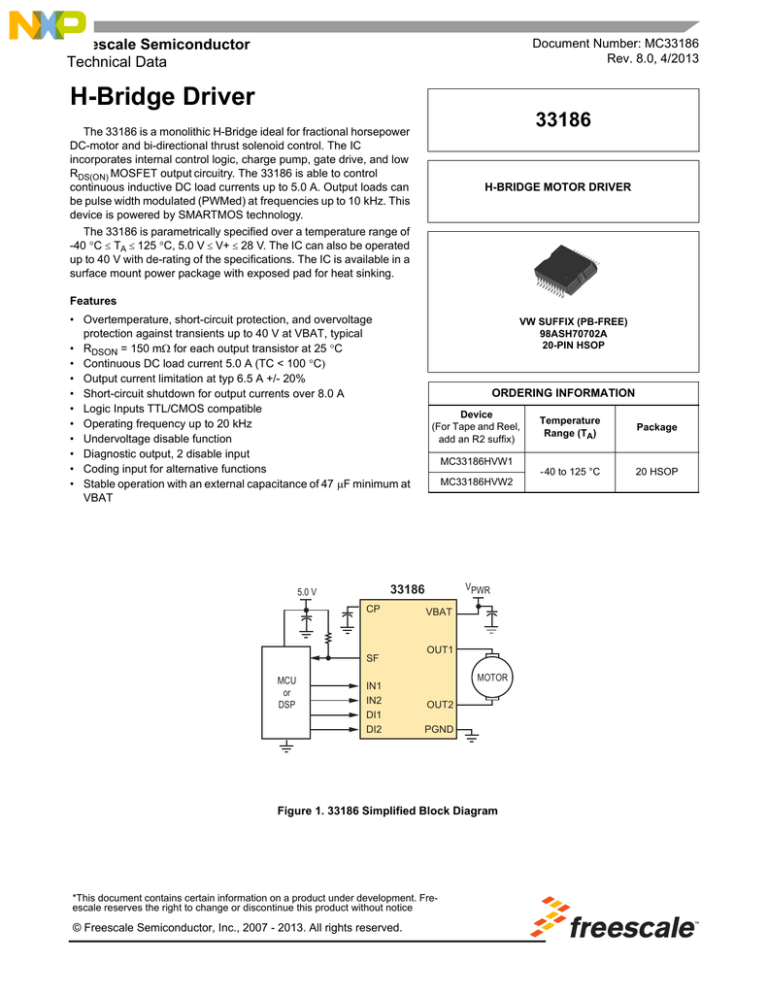
VPWR
33186
5.0 V
CP
SF
MCU
or
DSP
VW SUFFIX (PB-FREE)
98ASH70702A
20-PIN HSOP
IN1
IN2
DI1
DI2
VBAT
OUT1
MOTOR
OUT2
PGND
Figure 1. 33186 Simplified Block Diagram
*This document contains certain information on a product under development. Freescale reserves the right to change or discontinue this product without notice
© Freescale Semiconductor, Inc., 2007 - 2013. All rights reserved.
Temperature
Range (TA)
Package
- 40 to 125 °C
20 HSOP
INTERNAL BLOCK DIAGRAM
INTERNAL BLOCK DIAGRAM
CP
VBAT VBAT
VBAT
Internal 5.0 V
Charge-Pump
Undervoltage
SF
Overcurrent
High Side
Gate Control: 1-2
IN1
OUT1
IN2
Logic
Gate Control: 3-4
DI1
DI2
Overtemperature
COD
Current limitation
OUT2
Overcurrent
Current Limit
Low Side
PGND
Figure 2. 33186 Simplified Internal Block Diagram
33186
2
Analog Integrated Circuit Device Data
Freescale Semiconductor
PIN CONNECTIONS
PIN CONNECTIONS
Transparent Top View
Metal slug is connected
to power ground
AGND
SF
IN1
VBAT
VBAT
OUT1
OUT1
COD
PGND
PGND
1
2
3
4
5
6
7
8
9
10
20
19
18
17
16
15
14
13
12
11
NC
IN2
DI1
CP
VBAT
OUT2
OUT2
DI2
PGND
PGND
Figure 3. 33186 Pin Locations
Table 1. 33186 Pin Description
Pin
Name
9, 10, 11, 12
PGND
Power Ground. All the ground are connected together, they should be connected as short as
possible on the PCB.
1
AGND
Analog ground. All the ground are connected together, they should be connected as short as
possible on the PCB.
2
Output
Open drain output, active low. Is set according to the truth table. When a fault appears, SF changes
typically in less than 100 ms.
Metal slug
Status flag (SF)
3,13
Inputs IN1, IN2,
18, 19
DI1, DI2, COD
8
COD
Description
Voltage controlled inputs with hysteresis
When not connected or connected to GND, a stored failure will be reset by change of the voltagelevel on DI1 or DI2.
When connected to VCC, the disable Pin DI1 and DI2 are inactive. A stored failure will be reset by
change of the voltage level on IN1 or IN2.
6, 7, 14, 15
OUT1, OUT2
H-Bridge outputs with integrated freewheeling diodes.
33186
Analog Integrated Circuit Device Data
Freescale Semiconductor
3
PIN CONNECTIONS
Table 1. 33186 Pin Description(continued)
Pin
Name
Description
4, 5, 16
VBAT
The Pins 4 and 5 are internally connected. These Pins supply the left high side and the analog/logic
part of the device.
The Pin 16 supplies the right high side and the charge pump.
The Pins 4, 5 and 16 should be connected together on the printed circuit board with connections as
short as possible.
A VBAT filter capacitor, minimum value 47 F, should always be employed to prevent IC damage
from switching transients.
Supervision and protection functions
a) Supply voltage supervision
The supply voltage is supervised. If it is below its specific threshold, the power stages are switched
in tristate and the status flag is switched low.
If the supply voltage is over the specific threshold again, the power stage switches independently
into normal operation, according to the input Pins and the status flag is reset.
b) Thermal supervision
In case of overtemperature, the power stages are switched in tristate independent of the inputs
signals and the status flag is switched low.
If the level changes from high to low on DI1 (IN1) or low to high on DI2 (IN2), the output stage
switches on again if the temperature is below the specified limit.The status-flag is reset to high level
(Pin names in brackets refer to coding Pin = VCC).
c) Supervision of overcurrent on high sides and low sides
In case of overcurrent detection, the power stages are switched in tristate independent of the inputs
signals and the status flag is set.
If the level changes from high to low on DI1 (IN1) or low to high on DI2 (IN2) the output stage
switches on again and the status flag is reset to high level (Pin names in brackets refer to coding
Pin = VCC).
The output stage switches into the mode defined by the inputs Pins provided, and/if the temperature
is below the specified limits.
d) Current limiting on low sides
The maximum current which can flow under normal operating conditions is limited to Imax = 6.5 A
20%. When the maximum current value is reached, the output stages are switched tristate for a
fixed time. According to the time constant the current decreases until the next switch on occurs. See
page 9 for schematics.
17
CP
Charge Pump output Pin
A filtering capacitor (up to 33 nF) can be connected between Pin 17 and GND. Device can operate
without external capacitor, although Pin 17 decoupling capacitor help in noise reduction and allows
the device to perform a maximum speed, timing and PWM frequency.
33186
4
Analog Integrated Circuit Device Data
Freescale Semiconductor
ELECTRICAL CHARACTERISTICS
MAXIMUM RATINGS
ELECTRICAL CHARACTERISTICS
MAXIMUM RATINGS
Table 2. MAXIMUM RATINGS
All voltages are with respect to ground unless otherwise noted. Exceeding these ratings may cause a malfunction or
permanent damage to the device.
Ratings
Symbol
Min
Typ
Max
Unit
Static Destruction Proof
VBAT
- 1.0
–
28
Dynamic Destruction Proof t < 0,5 s
VBat
- 2.0
–
40
U
- 0.5
–
7.0
V
USF
- 0.5
–
7.0
V
Junction Temperature
TJ
- 40
–
+150
C
Storage Temperature
TS
- 55
–
+125
C
Ambient Temperature
TA
- 40
–
+125
C
–
–
+1.5
–
–
+1.5
ELECTRICAL RATINGS
Supply Voltage
Logic Inputs (IN1, IN2, DI1, DI2, CODE)
Output Status - Flag SF
V
THERMAL RATINGS
Thermal Resistance (with power applied on 2
power MOS)
RthJC
Thermal Resistance (with power applied on 2
power MOS)
RthJC
Peak Package Reflow Temperature During
Reflow (1), (2)
TPPRT
K/W
K/W
Note 2.
°C
Notes
1. Pin soldering temperature limit is for 10 seconds maximum duration. Not designed for immersion soldering. Exceeding these limits
may cause malfunction or permanent damage to the device.
2. Freescale’s Package Reflow capability meets Pb-free requirements for JEDEC standard J-STD-020C. For Peak Package Reflow
Temperature and Moisture Sensitivity Levels (MSL),
Go to www.freescale.com, search by part number [e.g. remove prefixes/suffixes and enter the core ID to view all orderable parts. (i.e.
MC33xxxD enter 33xxx), and review parametrics.
33186
Analog Integrated Circuit Device Data
Freescale Semiconductor
5
ELECTRICAL CHARACTERISTICS
STATIC ELECTRICAL CHARACTERISTICS
STATIC ELECTRICAL CHARACTERISTICS
Table 3. STATIC ELECTRICAL CHARACTERISTICS
Characteristic noted under conditions -40 C to +125 C, VBAT from 5.0 V to 28 V, unless otherwise note. Typical values
reflect approximate mean at 25 C, nominal VCC, at time of device characterization.
Characteristics
Symbol
Min
Typ
Max
5.0
–
–
–
28
–
–
35
Unit
POWER SUPPLY
Operating Range:
V
Static
VBAT
Dynamic (t < 500 ms)
VBAT
40
Stand-by current
f = 0 to 10 kHz; IOUT = 0.0 A
mA
I VBAT
VBAT-undervoltage switch-off (without load)
Switch-off Voltage
4.15
4.4
4.65
Switch-on Voltage
4.5
4.75
5.0
V
Hysteresis
150
–
–
mV
3.35
–
–
–
–
V
20
V
CHARGE-PUMP SUPPLY
VBAT = 4.15 V
VCP - VBAT
VBAT < 40 V
VCP - VBAT
LOGIC INPUTS
Input High
VINH
3.4
–
–
V
Input Low
VINL
–
–
1.4
V
Input Hysteresis
U
0.7
1.0
–
V
Input Pull-up Current (IN1, IN2, DI1)
I
- 200
- 80
–
A
IDI2
–
25
100
A
UIN = 0.0 V
Input Pull-down Current (DI2,COD)(3)
UDI2 = 5.0 V
POWER OUTPUTS: OUT1, OUT2
Switch on resistance:
m
ROUT - VBAT; ROUT - GND
VBAT = 5.0 to 28 V; CCP = 0 to 33 nF
–
–
300
Switch-off Current during Current Limitation
on Low Sides
(IOUT) MAX
5.2
6.5
7.8
A
Switch-off Time during Current Limitation on
Low Sides
tA
15
20.5
26
s
Blanking Time during Current Limitation on
Low Sides
tB
12
16.5
21
s
Notes
3. In case of negative voltage at OUT2 (respectively OUT1) this maximum pull down current at DI2 (respectively COD) Pin can be
exceeded. This happens during recirculation when the current is flowing in the low side. See Figure 22.
33186
6
Analog Integrated Circuit Device Data
Freescale Semiconductor
ELECTRICAL CHARACTERISTICS
STATIC ELECTRICAL CHARACTERISTICS
Table 3. STATIC ELECTRICAL CHARACTERISTICS(continued)
Characteristic noted under conditions -40 C to +125 C, VBAT from 5.0 V to 28 V, unless otherwise note. Typical values
reflect approximate mean at 25 C, nominal VCC, at time of device characterization.
Characteristics
Symbol
Min
Typ
Max
Unit
IOCHS
11
–
–
A
IOCLS
8.0
–
–
–
–
100
UD
–
–
2.0
tRR
–
2.0
5.0
Switch-off Temperature
160
–
190
Hysteresis
20
–
30
High Side Overcurrent Detection
(4)
Low Side Overcurrent Detection
Leakage Current
A
Output Stage Switched off
Freewheeling Diode Forward Voltage
IOU = 3.0 A
V
Freewheeling Diode Reverse
Recovery Time
s
IFM = 1.0 A, di/dt = 4.0 A/µs
C
OUTPUT STATUS FLAG (OPEN DRAIN OUTPUT)
Output High (SF not set)
USF = 5.0 V
A
ISF
–
–
10
VSF
–
–
1.0
f
–
–
10
Output Low (SF set)
ISF = 300 µA
V
TIMING
PWM frequency
CCP = 33 nF
kHz
Maximum Switching Frequency During
Current Limitation
VBAT = 6....28 V.....CCP = 33 nF
kHz
f
–
–
20
tDON
–
–
15
Output ON Delay
IN1.....>OUT1 or IN2.....>OUT2
s
Output OFF Delay
IN1.....>OUT1 or IN2.....>OUT2
s
tDOFF
–
–
15
Output Switching Time
s
CCP = 0 to 33 nF
OUTiH.....OUTiL, OUTiL.....OUTiH,
tr, tf
2.0
–
5.0
IOUT = 3.0 A
Disable Delay Time
DIi.....OUTi
s
–
–
8.0
Turn off in Case of Overcurrent or
Overtemperature
tDDIS
–
4.0
8.0
s
Power On Delay Time (CCP = 33 nF)(5)
–
1.0
5.0
ms
Notes
4. In case of overcurrent, the time when the current is greater than 7.8 A is lower than 30 s, with a maximum frequency of 1.0 kHz.
5. This parameter corresponds to the time for CCP to reach its nominal value when VBAT is applied.
33186
Analog Integrated Circuit Device Data
Freescale Semiconductor
7
ELECTRICAL CHARACTERISTICS
TRUTH TABLE
TRUTH TABLE
Table 4. Truth Table
Device State
Input Conditions
Status
Outputs
DI1 (8)
DI2 (8)
IN1
IN2
SF(9)
SF(10)
OU1
OU2
1-Forward
L
H
H
L
H
H
H
L
2-Reverse
L
H
L
H
H
H
L
H
3-Free Wheeling Low
L
H
L
L
H
H
L
L
4-Free Wheeling High
L
H
H
H
H
H
H
H
5-Disable 1
H
X
X
X
L
H
Z
Z
6-Disable 2
X
L
X
X
L
H
Z
Z
7-IN1 Disconnected
L
H
Z
X
H
H
H
X
8-IN2 Disconnected
L
H
X
Z
H
H
X
H
9-DI1 Disconnected
Z
X
X
X
L
H
Z
Z
10-DI2 Disconnected
X
Z
X
X
L
H
Z
Z
11-Current Limit.active
L
H
X
X
H
H
Z
Z
12-Undervoltage(6)
X
X
X
X
L
L
Z
Z
13-Overtemperature(7)
X
X
X
X
L
L
Z
Z
14-Overcurrent(7)
X
X
X
X
L
L
Z
Z
Notes
6. In case of undervoltage, tristate and status-flag are reset automatically.
7. Whenever overcurrent or overtemperature is detected, the fault is stored (i.e.status-flag remains low). The tristate conditions and the
status-flag are reset via DI1 (IN1) or DI2 (IN2). Pin names in brackets refer to coding Pin (COD = VCC).
8. If COD = VCC then DI1 and DI2 are not active.
9. COD = nc or GND
10. COD = VCC
L = Low
H = High
X = High or Low
Z = High impedance (all output stage transistors are switched off).
33186
8
Analog Integrated Circuit Device Data
Freescale Semiconductor
ELECTRICAL CHARACTERISTICS
TRUTH TABLE
10 k
47 µF
Ccp=33 nF
VBAT
Voltage
VCC
Regulator
Power Ground
SF
CP
VBAT
Micro controller
IN1
IN2
OUT1
M
DI1
OUT2
DI2
COD
GND
Power Ground
Figure 4. Typical Application
INn
50%
50%
tDON
OUn
tDOFF
90%
10%
Figure 5. Output Delay Time
DIn
50%
tDDIS
OUn
10%
Z
Figure 6. Disable Delay Time
33186
Analog Integrated Circuit Device Data
Freescale Semiconductor
9
ELECTRICAL CHARACTERISTICS
TRUTH TABLE
90%
90%
OUn
10%
tf
10%
tr
Figure 7. Output Switching Time
33186
10
Analog Integrated Circuit Device Data
Freescale Semiconductor
ELECTRICAL CHARACTERISTICS
TRUTH TABLE
Loadcurrent
Overturned
> 8A
TYP 6.5A
A
Control
signal
Status
Flag
Overcurrent detection
Detail A
tA
6.5A
tB
tA = switch-off time in current limitation
tB = current limitation blanking time
Figure 8. Current Limitation on Low Side
33186
Analog Integrated Circuit Device Data
Freescale Semiconductor
11
ELECTRICAL CHARACTERISTICS
TRUTH TABLE
13,5
2,83
13
2,82
2,81
12
2,80
11,5
VinH (V)
IVBAT (mA)
12,5
11
10,5
VBAT=12V
10
2,78
2,77
9,5
9
-50
2,79
2,76
-25
0
25
50
75
T, TEMPERATURE (C)
100
2,75
-50
125
Figure 9. Stand-by Current vs. Temperature
-25
0
25
50
75
T, TEMPERATURE (C)
100
125
Figure 12. High Threshold Input Voltage vs.
Temperature
5,00
45
4,90
4,70
35
4,60
30
4,50
4,40
Switch off Voltage
without Ccp
25
20
15
4,30
4,20
-50
Tambient=25°C
40
Switch on Voltage
Vcp (V)
VBAT(V)
4,80
10
-25
0
25
50
75
T, TEMPERATURE (C)
100
125
5
0
Figure 10. VBAT Undervoltage vs. Temperature
5
0
1,88
200
1,87
190
1,86
35
VBAT=5V without Ccp
180
1,85
RDSON (m)
VinL (V)
30
Figure 13. Vcp vs. Battery Voltage
1,89
1,84
1,83
1,82
1,81
-50
10
15
20
25
BATTERY VOLTAGE (V)
170
160
150
140
130
-25
0
25
50
75
T, TEMPERATURE (C)
100
125
Figure 11. Low Threshold Input Voltage vs. Temperature
120
110
-50
-25
0
25
50
75
100
125
T, TEMPERATURE (C)
Figure 14. RDSON vs. Temperature
33186
12
Analog Integrated Circuit Device Data
Freescale Semiconductor
ELECTRICAL CHARACTERISTICS
TRUTH TABLE
ta=20.5µs
7,20
7,10
Imotor (1A/div)
IOUT max (A)
7,00
6,90
Out1 (5V/div)
6,80
6,70
6,60
6,50
Out2 (5V/div)
6,40
6,30
-50
-25
0
25
50
75
100
125
T, TEMPERATURE (C)
Figure 18. Switch off Time
Figure 15. Switch off Current vs. Temperature
17,50
17,00
IOCHS (A)
16,50
16,00
Out1 (5V/div)
High side switch
15,50
15,00
14,50
14,00
13,50
13,00
-50
tr=3.7µs
-25
0
25
50
75
100
125
Figure 19. Output Switching Time: TR
T, TEMPERATURE (C)
Figure 16. Overcurrent Detection vs. Temperature
I(out) max= 7A
Out1 (5V/div)
Imotor (1A/div)
tf=2.6µs
Figure 20. Output Switching Time: TF
Figure 17. Current Limitation
33186
Analog Integrated Circuit Device Data
Freescale Semiconductor
13
ELECTRICAL CHARACTERISTICS
TRUTH TABLE
in1 (1V/div)
I(5A/div)
Out1 (2V/div)
Iochs= 16A
tdoff=12.5µs
Figure 21. Output OFF Delay
Figure 24. High Side Overcurrent High Side Detection
3.2
3
2.8
2.6
tdon=5.8µs
2.4
2.2
2
Out1 (2V/div)
1.8
1.6
1.4
1.2
in1 (1V/div)
1
0.8
0.6
0.4
Figure 22. Output ON Delay
0.2
0
0
1
2
3
4
5
6
7
8
9
10
11 12
13 14
15 16
17 18
19 20
I OUT2 (A)
di2 (1V/div)
Note: Current through internal recirculation diode, @125°C in case of
negative voltage at OUT2
Out1 (2V/div)
Figure 25. Maximum Di2 Input Current vs. IOUT2, current
tdiss=0.9µs
Figure 23. Disable Delay Time
33186
14
Analog Integrated Circuit Device Data
Freescale Semiconductor
PACKAGING
SOLDERING
PACKAGING
SOLDERING
The 20 HSOP package is designed for enhanced thermal
performance. The particularity of this package is its copper
base plate on which the power die is soldered. The base plate
is soldered on a PCB to provide heat flow to the ambient and
also to provide a large thermal capacitance.
Of course, the more copper area on the PCB, the better
the power dissipation and transient behavior.
We characterized the 20 HSOP on a double side PCB.
The bottom side area of the copper is 7.8 cm2. The top
surface is 2.7 cm2, see Figure 26.
100
10
Rth (°C/W)
1
0,1
0,001
0,01
0,1
1
10
t, Time (s)
100
1000
10000
Figure 27. PHSOP20 Thermal Response
Figure 27 shows the thermal response with the device
soldered on to the test PCB described on Figure 26.
Top Side
Bottom Side
Figure 26. PCB Test Layout
33186
Analog Integrated Circuit Device Data
Freescale Semiconductor
15
PACKAGING
PACKAGE DIMENSIONS
PACKAGE DIMENSIONS
Important: Package dimensions are provided in package drawings. To find the most current package outline drawing, go to
www.freescale.com and perform a keyword search for the drawing’s document number.
Table 5. Package Drawing Information
Package
Suffix
Package Outline Drawing Number
20-PIN HSOP
HVW
98ASH70702A
Dimensions shown are provided for reference ONLY (For Layout and Design, refer to the Package Outline Drawing listed in
the following figures).
33186
16
Analog Integrated Circuit Device Data
Freescale Semiconductor
PACKAGING
PACKAGE DIMENSIONS
VW (Pb-FREE) SUFFIX
20-PIN HSOP
98ASH70702A
ISSUE C
33186
Analog Integrated Circuit Device Data
Freescale Semiconductor
17
PACKAGING
PACKAGE DIMENSIONS
VW (Pb-FREE) SUFFIX
20-PIN HSOP
98ASH70702A
ISSUE C
33186
18
Analog Integrated Circuit Device Data
Freescale Semiconductor
PACKAGING
PACKAGE DIMENSIONS
VW (Pb-FREE) SUFFIX
20-PIN HSOP
98ASH70702A
ISSUE C
33186
Analog Integrated Circuit Device Data
Freescale Semiconductor
19
ADDITIONAL DOCUMENTATION
THERMAL ADDENDUM (REV 2.0)
ADDITIONAL DOCUMENTATION
33186VW
THERMAL ADDENDUM (REV 2.0)
Introduction
20-PIN
HSOP-EP
This thermal addendum is provided as a supplement to the MC33186 technical
datasheet. The addendum provides thermal performance information that may be
critical in the design and development of system applications. All electrical,
application, and packaging information is provided in the datasheet.
Package and Thermal Considerations
The MC33186 is offered in a 20 pin HSOP exposed pad, single die package.
There is a single heat source (P), a single junction temperature (TJ), and thermal
resistance (RJA).
VW SUFFIX (Pb-FREE)
98ASH70273A
20-PIN HSOP-EP
Note For package dimensions, refer to
the 33186 data sheet.
TJ
=
RJA
.
P
The stated values are solely for a thermal performance comparison of one
package to another in a standardized environment. This methodology is not
meant to and will not predict the performance of a package in an applicationspecific environment. Stated values were obtained by measurement and
simulation according to the standards listed below.
Standards
Table 6. Thermal Performance Comparison
Thermal Resistance
[C/W]
(1), (2)
29
RJB (2), (3)
9.0
RJA (1), (4)
69
RJC (5)
2.0
RJA
Notes:
1. Per JEDEC JESD51-2 at natural convection, still air condition.
2. 2s2p thermal test board per JEDEC JESD51-5 and
JESD51-7.
3. Per JEDEC JESD51-8, with the board temperature on the
center trace near the center lead.
4. Single layer thermal test board per JEDEC JESD51-3 and
JESD51-5.
5. Thermal resistance between the die junction and the exposed
pad surface; cold plate attached to the package bottom side,
remaining surfaces insulated.
1.0
0.2
1.0
0.2
* All measurements
are in millimeters
Soldermast
openings
20 Pin HSOP-EP
1.6 mm Pitch
16.0 mm x 11.0 mm Body
12.3 mm x 7.1 mm Exposed Pad
Thermal vias
connected to top
buried plane
Figure 28. Thermal Land Pattern for Direct Thermal
Attachment According to JESD51-5
33186
20
Analog Integrated Circuit Device Data
Freescale Semiconductor
ADDITIONAL DOCUMENTATION
THERMAL ADDENDUM (REV 2.0)
A
AGND
SF
IN1
VBAT
VBAT
OUT1
OUT1
COD
PGND
PGND
20
19
18
17
16
15
14
13
12
11
1
2
3
4
5
6
7
8
9
10
NC
IN2
DI1
CP
VBAT
OUT2
OUT2
DI2
PGND
PGND
33186VW Pin Connections
20-Pin HSOP-EP
1.6 mm Pitch
16.0 mm x 11.0 mm Body
12.3 x 7.1 mm exposed pad
Figure 29. Thermal Test Board
Device on Thermal Test Board
Material:
Outline:
Single layer printed circuit board
FR4, 1.6 mm thickness
Cu traces, 0.07 mm thickness
80 mm x 100 mm board area,
including edge connector for
thermal testing
Area A:
Cu heat-spreading areas on board
surface
Ambient Conditions:
Natural convection, still air
Table 7. Thermal Resistance Performance
A [mm2]
RJA [C/W]
0
70
300
49
600
47
RJAis the thermal resistance between die junction and
ambient air.
33186
Analog Integrated Circuit Device Data
Freescale Semiconductor
21
ADDITIONAL DOCUMENTATION
THERMAL ADDENDUM (REV 2.0)
Thermal
Resistance [ºC/W]
Thermal Resistance [C/W]
80
80
70
70
60
60
50
50
40
40
30
30
20
20
x
10
10
00
00
RJA [°C/W]
300
300
Heat spreading area A [mm²]
Heat Spreading Area A [mm2]
600
600
Figure 30. Device on Thermal Test Board RJA
Thermal Resistance [C/W]
Thermal Resistance [ºC/W]
100
100
10
10
x
1
RJA [°C/W]
0.1
0.1
1.00E-03
1.00E-03
1.00E-02
1.00E-02 1.00E-01
1.00E-01
1.00E+00 1.00E+01
1.00E+03 1.00E+04
1.00E+00
1.00E+01 1.00E+02
1.00E+02 1.00E+03
1.00E+04
Time [s]
Time[s]
Figure 31. Transient Thermal Resistance RJA
1 W Step Response, Device on Thermal Test Board Area A = 600 (mm2)
33186
22
Analog Integrated Circuit Device Data
Freescale Semiconductor
REVISION HISTORY
REVISION HISTORY
REVISION
DATE
DESCRIPTION OF CHANGES
5.0
5/2006
•
•
Implemented Revision History page
Added Lead Free (Pb-Free) Part Number MC33186VW1
6.0
10/2006
•
•
Updated data sheet formal
Removed Peak Package Reflow Temperature During Reflow (solder reflow) parameter from
MAXIMUM RATINGS on page 5. Added note with instructions to obtain this information from
www.freescale.com.
7.0
10/2011
•
Updated Package Dimensions according to the latest Freescale package specification
98ASH70702A_C
Updated to the current Freescale form and style.
8.0
4/2013
•
•
•
•
Removed MC33186DH1 and MC33186VW1 from the ordering information and added
MC33186HVW1 and MC33186HVW2 to the ordering information
Added the sentence “A VBAT filter capacitor, minimum value 47 F, should always be employed to
prevent IC damage from switching transients.” for pins 4,5 , and 16 in Table 1
Revised back page. Updated document properties. Added SMARTMOS sentence to first
paragraph. Updated form and style.
33186
Analog Integrated Circuit Device Data
Freescale Semiconductor
23
How to Reach Us:
Information in this document is provided solely to enable system and software implementers to use Freescale products.
Home Page:
freescale.com
There are no express or implied copyright licenses granted hereunder to design or fabricate any integrated circuits on
Web Support:
freescale.com/support
Freescale reserves the right to make changes without further notice to any products herein. Freescale makes no
the information in this document.
warranty, representation, or guarantee regarding the suitability of its products for any particular purpose, nor does
Freescale assume any liability arising out of the application or use of any product or circuit, and specifically disclaims any
and all liability, including without limitation consequential or incidental damages. “Typical” parameters that may be
provided in Freescale data sheets and/or specifications can and do vary in different applications, and actual performance
may vary over time. All operating parameters, including “typicals,” must be validated for each customer application by
customer’s technical experts. Freescale does not convey any license under its patent rights nor the rights of others.
Freescale sells products pursuant to standard terms and conditions of sale, which can be found at the following address:
http://www.reg.net/v2/webservices/Freescale/Docs/TermsandConditions.htm
Freescale and the Freescale logo, are trademarks of Freescale Semiconductor, Inc., Reg. U.S. Pat. & Tm. Off.
SMARTMOS is a trademark of Freescale Semiconductor, Inc. All other product or service names are the property of their
respective owners.
© 2013 Freescale Semiconductor, Inc.
Document Number: MC33186
Rev. 8.0
4/2013
