Advances in Computing 2013, 3(3): 73-84
DOI: 10.5923/j.ac.20130303.06
A Novel High Accuracy Digital Lock Detector with False
Lock Detection
Muhammad Azhar Mohamed Sherafath Ali*, Zulfiqar Ali Abdul Aziz
School of Electrical & Electronic Engineering, Universiti Sains Malaysia, Nibong Tebal, 14300, Malaysia
Abstract The purpose of this paper is to introduce a new circuit into the traditional DLL to define the lock condition.
Fully digital lock detector is presented where the design is simple and process independence. The lock detector consists of
two main blocks, LOCK INDICATOR and CORRECT LOCK INDICATOR. The lock detector has been integrated with an
8-phase DLL and a circuit simulation has been done. Compare to conventional lock detector circuit, the proposed lock
detector can detect false lock (when CLKOUT and CLKREF is 180° out of phase) by just using an X-OR gate. The proposed
circuit also compares both the positive and negative cycle of the CLKREF and CLKOUT; hence the detection is more
accurate. By using this lock detection method, the lock detector can detect down to 2ps phase offset between the CLKREF
and CLKOUT. The CORRECT LOCK INDICATOR block is introduced to detect whether the CLKOUT is locked to the
CLKREF by exactly one clock cycle. Hence, this block also serves as false lock detector.
Keywords DLL, Novel High Accuracy Digital Lock Detector, Detection down to 2ps phase offset
1. Introduction
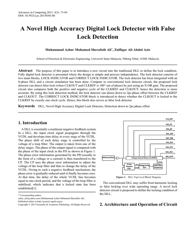
A DLL is essentially a nonlinear negative feedback system.
In a DLL, the input clock signal propagates through the
VCDL and develops time delay at every stage of the VCDL.
The phase shift of each delay stage is controlled by the
voltage of a loop filter. The output is taken from one of the
delay stages. The phase of the output signal is compared with
the phase of the input clock in the PD as shown in Figure 1.
The phase error information generated by the PD (usually in
the form of a voltage or a current) is then transferred to the
CP. The CP uses the phase error information to adjust the
voltage of the loop filter and thus to change the delay of the
VCDL. Owing to such a negative feedback mechanism, the
phase error is gradually reduced until it finally becomes zero.
At that time, the delay of the whole VCDL line becomes
equal to one clock period, and the voltage of the loop filter is
stabilized, which indicates that a locked state has been
established[1].
* Corresponding author:
azhar_als@yahoo.com (Muhammad Azhar Mohamed Sherafath Ali)
Published online at http://journal.sapub.org/ac
Copyright © 2013 Scientific & Academic Publishing. All Rights Reserved
Figure 1. DLL Top Level Block Diagram
The conventional DLL may suffer from harmonic locking
or false locking over wide operating range. A novel lock
detector circuit is proposed to define the locking condition of
the DLL.
2. Architecture and Operation of Circuit
74
Muhammad Azhar Mohamed Sherafath Ali et al.: A Novel High Accuracy
Digital Lock Detector with False Lock Detection
Figure 2. DLL Top Level with the Lock Detector
Figure 3 shows the proposed LOCK DETECTOR top level schematic. It consists of LOCK INDICATOR block and
CORRECT LOCK INDICATOR block.
Figure 3. Top Level Schematic of the Proposed Lock Detector
2.1. Lock Indicator Block
The LOCK INDICATOR block accepts both the CLKREF and CLKOUT and compares them. It will indicate whether or
not the CLKOUT is exactly locked to the CLKREF. The CORRECT LOCK INDICATOR block accept the other 6 phase
clocks (CLK45, CLK90, CLK135, CLK180, CLK225, CLK270 and CLK315) and indicates whether or not the CLKOUT is
delayed from the CLKREF by exactly one clock cycle. The final output (LOCK) will only toggle to ‘1’ only and if only both
of the conditions are satisfied (the output of LOCK INDICATOR and CORRECT LOCK INDICATOR must toggle to ‘1’).
Figure 4 shows the LOCK INDICATOR block schematic.
Advances in Computing 2013, 3(3): 73-84
75
Figure 4. Lock Indicator Block Schematic
Figure 5. LOCK# block schematic
The LOCK# block will indicate whether the CLKREF and CLKOUT are locked (both their positive and negative cycles
are exactly in line). It will do so by comparing the rising edge and the falling edge of the CLKOUT with the CLKREF. When
the CLKOUT and the CLKREF are locked, both the rising edge DFF and falling edge DFF will toggle to ‘1’. Hence, when the
CLKOUT and CLKREF are exactly in line, the output (OUT1) will be ‘0’.
76
Muhammad Azhar Mohamed Sherafath Ali et al.: A Novel High Accuracy
Digital Lock Detector with False Lock Detection
Figure 6. Output waveforms when CLKOUT is locked to CLKREF
If the system is not locked and CLKOUT delay is less than 1 clock cycle from the CLKREF, the rising edge DFF will
toggle to ‘1’ and the falling edge DFF will remain ‘0’. Hence, when the CLKOUT and CLKREF are not in line, the OUT1
will be ‘1’.
Figure 7. Output waveforms when CLKOUT is delayed less than 1 clock-cycle from the CLKREF
Advances in Computing 2013, 3(3): 73-84
77
If the system is not locked and CLKOUT delay is more than 1 clock cycle from CLKREF, the falling edge DFF will toggle
to ‘1’ and the rising edge DFF will remain ‘0’. Hence, the OUT1 will also be ‘1’. So when the OUT1 is at ‘1’, the CLKOUT
and CLKREF are not in line.
Figure 8. Output waveforms when the CLKOUT is delayed more than 1 clock-cycle from the CLKREF
There will be case where the LOCK DETECTOR may give wrong indication. This is when the CLKOUT and CLKREF
are exactly 180 phase shift as shown below.
Figure 9. Output waveforms when CLKOUT and CLKREF is 180° out of phase
78
Muhammad Azhar Mohamed Sherafath Ali et al.: A Novel High Accuracy
Digital Lock Detector with False Lock Detection
During this condition, both the rising edge DFF and falling edge DFF will toggle ‘1’ and the OUT1 will be’0’. The lock
detector will indicate the system is locked although CLKOUT and CLKREF are not locked actually. We want to avoid this
problem. A circuit is needed to detect this phenomenon as a false lock. So we pass both the CLKREF and CLKOUT through
an X-OR gate as shown in Figure 10 below.
Figure 10. Circuitry to avoid false lock detection when CLKOUT and CLKREF are 180° out of phase. Both the CLKREF and CLKOUT are passed
through the X-OR gate
So if the CLKREF and CLKOUT are exactly 180 out of phase, the X-OR gate will produce a ‘1’ and the DFF2 and DFF3
(shown in Figure 10) will toggle to ‘1’. Hence the final output, OUT2 will be ‘0’ indicating that the CLKREF and CLKOUT
are not in phase although OUT1 toggles to ‘0’ as shown in Figure 11 below.
Figure 11. Output waveforms after using the additional circuitry. OUT2 is ‘0’ indicating CLKREF and CLKOUT are not in phase
Advances in Computing 2013, 3(3): 73-84
79
When the CLKREF and CLKOUT are exactly in phase, the X-OR gate will output a ‘0’ and the DFF2 and DFF3 will
toggle to ‘0’. The OUT1 will be ‘0’. Hence the final output, OUT2 will be ‘1’ indicating that CLKREF and CLKOUT are
exactly in phase.
Figure 12. Output waveforms when CLKREF and CLKOUT exactly in phase
Hence, the X-OR gate with some additional circuitry acts as false lock detector when the CLKOUT is 180° out of phase
from the CLKREF. The OUT2 will only toggle to ‘1’ when CLKOUT is exactly locked to CLKREF.
2.2. Correct Lock Indicator Block
This block indicates whether the CLKOUT and CLKREF are locked correctly or not. In another word, this block will
detect whether the CLKOUT is locked to CLKREF by 1 clock cycle delay. There will be cases where the CLKOUT is locked
to CLKREF by 2 clock cycles or more. During the situation, the LOCK INDICATOR block will indicate the DLL is locked.
This is also a false lock phenomenon as shown in Figure 13 below. In this example, the CLKOUT is locked to CLKREF by 2
clock cycles.
Figure 13. Output waveforms when CLKOUT is locked to CLKREF by 2 clock cycles
80
Muhammad Azhar Mohamed Sherafath Ali et al.: A Novel High Accuracy
Digital Lock Detector with False Lock Detection
The OUT2 will toggle to ‘1’ indicating that the CLKOUT is locked to the CLKREF, but this is false lock phenomenon.
To avoid this problem we design a block called CORRECT LOCK INDICATOR. This block indicates whether the
CLKOUT and CLKREF are locked correctly or false locked. In another word, this block will detect whether the CLKOUT is
locked to CLKREF by 1 clock cycle delay. Figure below shows the CORRECT LOCK INDICATOR block for 8-phase DLL.
Figure 14. CORRECT LOCK INDICATOR Block Schematic
The output of this block, OUT3 will be AND with the output of the LOCK INDICATOR block, OUT2 as shown in the top
level schematic below.
Figure 15. Lock Detector Top Level Schematic
Advances in Computing 2013, 3(3): 73-84
81
The final output (LOCK), will only toggle to ‘1’ if the OUT3 is ‘1’ and the OUT2 is ‘1’. In another words, the final output
will only indicate that the DLL is locked only if the CLKOUT is delayed exactly by one clock cycle from CLKREF.
3. Results
3.1. Lock Detector Simulation Result
Figure 16 below shows the condition where the CLKOUT is locked to CLKREF by 1 clock cycle. The output from LOCK
INDICATOR block, OUT2 toggles to ‘1’. The output from CORRECT LOCK INDICATOR block, OUT3 also toggles to ‘1’
and remains. When this condition is met, the final output of the LOCK DETECTOR block, LOCK will toggle to ‘1’ and
indicates that the DLL is locked correctly.
Figure 16. Output waveforms when DLL is locked. All the 8 phase clocks are separated 260.4ps harmonically. The LOCK pin toggles to ‘1’ indicating the
DLL is locked
Figure 17 shows the condition where the CLKOUT is locked to the CLKREF by 2 clock cycle. We can see that the LOCK
INDICATOR output, OUT2 toggles to ‘1’ because the CLKOUT is locked to the CLKREF, but the CORRECT LOCK
INDICATOR remains at ‘0’, indicating that CLKOUT is not locked by 1 clock cycle to the CLKREF. Hence the final output,
LOCK stays at ‘0’, indicating that the DLL system in not locked.
82
Muhammad Azhar Mohamed Sherafath Ali et al.: A Novel High Accuracy
Digital Lock Detector with False Lock Detection
Figure 17. Output waveforms when DLL is not locked. All the 8 phase clocks are separated 520.8ps harmonically. The lock pin remains ‘0’ indicating the
DLL is not locked
Figure 18 shows the waveform where the CLKOUT is locked to the CLKREF by 3 clock cycle delay. The LOCK
DETECTOR will indicate that the DLL is not locked.
Figure 18. Output waveforms when DLL is not locked. All the 8 phase clocks are separated 1041.6ps harmonically. The lock pin remains ‘0’ indicating the
DLL is not locked
Advances in Computing 2013, 3(3): 73-84
83
3.2. DLL Top Level Simulation Result
The LOCK DETECTOR is integrated with the 8-phase DLL as shown in the top level schematic in Figure 19 below.
Figure above shows the 8 phase clocks signal generated from the DLL and the LOCK signal from the LOCK DETECTOR.
The locking time is 71.15n.
Figure 19. DLL Top Level Schematic
Figure 20. Output waveforms generated by the DLL together with the Lock Detector
84
Muhammad Azhar Mohamed Sherafath Ali et al.: A Novel High Accuracy
Digital Lock Detector with False Lock Detection
4. Conclusions
ACKNOWLEDGMENTS
A new digital lock detector has been proposed, where the
LOCK INDICATOR and CORRECT LOCK INDICATOR
serve as false lock detector when the CLKOUT is 180° out of
phase from CLKREF, and when the CLKOUT is locked to
the CLKREF more than 1 clock cycle, respectively. A very
accurate lock detection scheme (down to 2ps phase offset) is
achieved by comparing both the positive and negative cycle
of the feedback clock (CLKOUT) with the reference clock
(CLKREF), and by using less amount of components to
avoid unnecessary delay. The other advantages of this digital
lock detector are its process independence and design
simplicity.
Academicals support from Science University of Malaysia
is gratefully acknowledged.
REFERENCES
[1]
C. JIA, “A Delay-Locked Loop for Multiple Clock
Phases/Delays Generation, Doctoral Thesis, Georgia Institute
of Technology, 2005.


