Application Note
Network
Communications
Physical Layer
Testing with a
CSA7000 Series
Communications
Signal Analyzer
Physical layer testing of electrical and optical telecom and
datacom signals up to 2.5 Gb/s.
The CSA7000 Series real-time communications signal analyzer provides the versatility needed
to test design outputs for standard compliance and to analyze critical circuit parameters.
In designing wired communications network equipment, a key
element of signal testing is testing the equipment’s physical layer.
The physical layer is the lowest layer in the Open Systems
Interconnection (OSI) network model. Today’s high-performance
digital phosphor oscilloscopes (DPOs), such as the CSA7000 Series
communications signal analyzer, have the electrical and optical
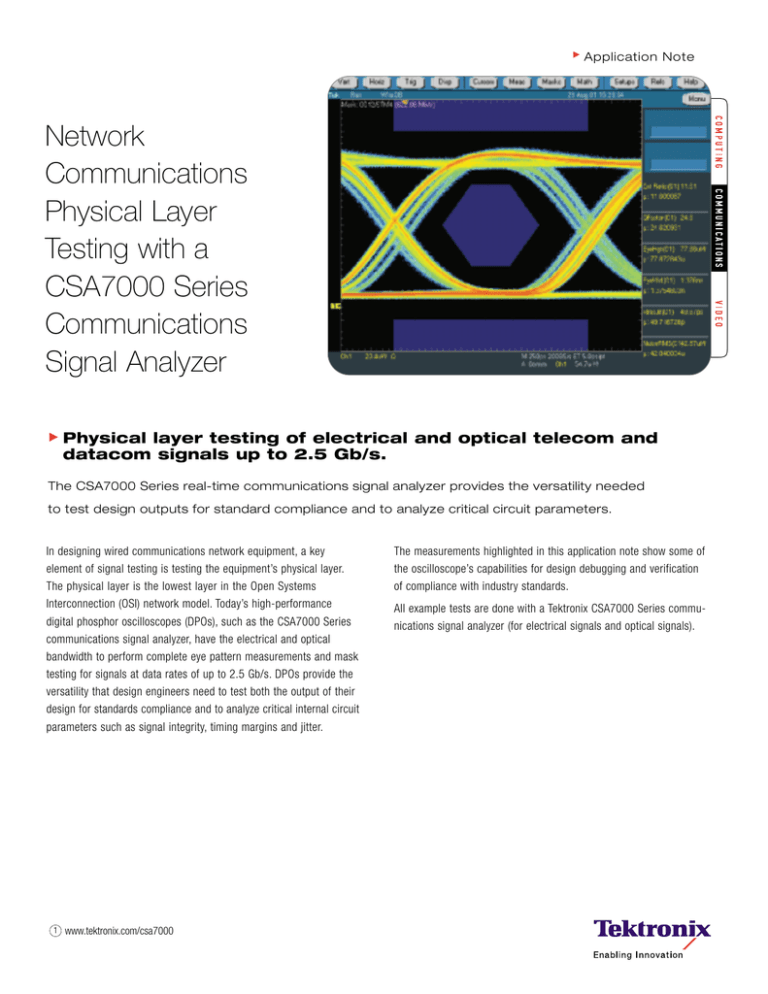
bandwidth to perform complete eye pattern measurements and mask
testing for signals at data rates of up to 2.5 Gb/s. DPOs provide the
versatility that design engineers need to test both the output of their
design for standards compliance and to analyze critical internal circuit
parameters such as signal integrity, timing margins and jitter.
1
www.tektronix.com/csa7000
The measurements highlighted in this application note show some of
the oscilloscope’s capabilities for design debugging and verification
of compliance with industry standards.
All example tests are done with a Tektronix CSA7000 Series communications signal analyzer (for electrical signals and optical signals).
Network Communications Testing with a CSA7000 Series
Application Note
Ta b l e 1 . W i r e d C o m m u n i c a t i o n s N e t w o r k P h y s i c a l L a y e r
Specifications Covered in this Application Note
SONET/SDH GR 253-CORE
OC-1/STM0
OC-3/STM1
OC-12/STM4
OC-48/STM16
ITU-T G.703
DS1 Rate, DS2 Rate Sym Pair,
DS2 Rate Coax, DS3 Rate
E1 Sym Pair, E1 Coax, E2, E3
E4 Binary 0, E4 Binary 1
32 Mb, 97 Mb
STM 1E 0/ Bin 0, STM 1E 1/ Bin 1
ANSI T1.102-1993
DS1, DS1A, DS1C, DS2, DS3,
DS4NA, DS4NA Max Output
STS-1 Pulse, STS-1 Eye
STS-3, STS-3 Max Output
Ethernet IEEE Std 802.3 and ANSI X3.263-1995
100 Base-T STP, 100 Base-T UTP
1000 Base-SX Short Wave Optical
1000 Base-LX Long Wave Optical
Fibre Channel Optical
FC133, FC266, FC531,
FC1063, FC1063 Draft Rev 11
FC2125
Fibre Channel Electrical
FC133E, FC266E, FC531E
FC1063E
FC1063E Normalized Beta, Delta, Gamma Transmit
FC1063E Absolute Beta, Delta, Gamma Transmit
FC1063E Absolute Beta, Delta, Gamma Receive
FC2125E Normalized Beta, Delta, Gamma Transmit
FC2125E Absolute Beta, Delta, Gamma Transmit
C2125E Absolute Beta, Delta, Gamma Receive
USB 1.1 / 2.0
FS:T1, T2, T3, T4, T5, T6
HS:T1, T2, T3, T4, T5, T6
InfiniBand
2.5 Gb/s Optical
IEEE1394
S400ß Optical
2.5 Gb/s Electrical
S400ß T1, S400ß T2
S800ß Optical
S800ß T1, S800ß T2
S1600ß Optical
S1600ß T1, S1600ß T2
Serial ATA
G1, G1 Rx, G1 Tx
G2, G2 Rx, G2 Tx
2
www.tektronix.com/csa7000
Network Communications Testing with a CSA7000 Series
Application Note
Design Debug with a DPO
Wired communications network equipment must not only meet performance specifications, but also conform to industry standards, and
offer interoperability between various standards. When designing and
debugging these very complex systems, insight into signal interaction
and behavior is critical. For example, when designing a communications
transmitter, engineers need to capture intermittent failures that can
occur and observe the device’s output to determine if its parameters
are within acceptable limits.
Today’s high-performance DPOs, such as the CSA7000 Series communications signal analyzer, allow users to observe high data rate signals
such as OC-48/STM-16. In addition, their real-time acquisition captures
many infrequent events that sampling oscilloscopes would miss.
Sampling oscilloscopes acquire data using one point per trigger, and
therefore use hundreds of triggers in order to build a waveform. This
low duty cycle acquisition works well for high data rate signals whose
characteristics are repetitive. However, the time required to acquire
enough waveform data using a sampling oscilloscope reduces the
possibility of capturing infrequent events.
A high-performance DPO is a valuable companion to the BERT
because its intensity-graded display enables the user to observe
a transmitter’s output and immediately see if there are intermittent
problems. For example, a common technique for isolating intermittent
problems is to use an analyzer to trigger on a network event. The
event usually is a network error condition—an occurrence of a certain
frame or a network statistic reaching a certain level. The problem
can also be pattern dependent and generates a spike on the output
transmitter or jitter. These types of problems can cause intermittent
signal loss as well as total link failures that are not easily caught by a
sampling scope or even a BERT. The advanced triggering available in
a DPO allows quick location of signal errors. The TDS7000 Series and
CSA7000 Series DPOs offer several categories of advanced triggers
including communications logic triggering, pulse width triggering, and
unique serial pattern triggering.
For communications hardware debugging at rates up to 2.5 Gb/s,
a real-time oscilloscope is often the best test instrument. When a
transmitter is not working or is only "partially" working, a real-time
oscilloscope is invaluable for debugging the design. The DPO graphical
display makes finding the problem easier. If the design is not working,
a bit error rate tester (BERT) alone cannot help a designer determine
the source of the problem. A BERT can be very effective in finding
errors that occur very infrequently, but only if the communication
device under test is working well enough to accept inputs and/or
transmit data. The BERT transmitter outputs a known data pattern to
stimulate the device-under-test. The BERT receiver accepts the device’s
output data and looks for bit errors to occur. The BERT receiver typically
only has a numeric display that shows bit error rate.
www.tektronix.com/csa7000 3
Network Communications Testing with a CSA7000 Series
Application Note
Standards Verification
For network equipment to be accepted by the industry it must comply
with industry telecom standards such as SONET/SDH, ANSI T1.105,
ITU-T G. or datacom standards including IEEE802.3 and ANSI T11.2.
These standards specify physical layer characteristics and measurement
conditions such as the following.
Electrical specifications: The 1000 BASE-CX transmitter specifications
define data rate, clock tolerance, nominal signaling speed, differential amplitude, rise/fall time and differential skew. They also include an eye diagram
requirement when measured in a specified transmitter test load.
Eye diagram shape specifications: The minimum eye openings at the Fibre
Channel receiver is only about 200 ps wide for FC2125.
Optical specifications: SONET optical measurements require an ORR (optical
reference receiver) with a Bessel-Thompson characteristic. Optical Fibre
Channel requires the same filter, an 850 nm wavelength optical receiver and
clock recovery from the data. For most standards, a variety of measurements
in the time domain are taken to characterize the shape of the waveform
being transmitted. These measurements include period, rise time, fall time,
clock-to-data jitter, extinction ratio, Q-factor, crossing %, eye height, eye
width and duty cycle distortion
Jitter specifications: Fibre channel is the originator of random, deterministic
and total jitter. The measurements must be made differentially (if differential
electrical), because asymmetries in the electrical signaling or the physical
PCB traces add jitter.
BER specifications: The InfiniBand specification calls for eye diagram and
jitter tests to ensure a low bit error rate (BER).
Figure 1. An example of each type of mask.
Mask Testing Requirements
One of the key requirements for testing telecom equipment is the ability
to guarantee interoperability of equipment from various vendors. Mask
testing was developed with this requirement in mind. Mask testing can
ensure that most of the key wave shape parameters (period, rise/fall
times, clock-to-data jitter, overshoot, ringing, noise, signal to noise
ratio) are within acceptable tolerances. Because the shape of the
measured waveform is dependent on the frequency response (i.e.
bandwidth) of the measurement system, the standards bodies have
specified a standard "reference receiver" which should be used for
these measurements. By tightly controlling the frequency response of
the measurement system (via the use of a standard reference receiver),
repeatability of measurements between various test and measurement
vendors equipment can be guaranteed.
A mask that defines the region where the signal must reside on the
oscilloscope’s display specifies the eye diagram mask test. These
masks vary by the type of signal being tested. For many of the lower
data rate electrical signals, a mask for a single positive or negative
pulse is defined. For the high-speed electrical and optical signals,
an eye diagram mask is defined (Figure 1).
4
www.tektronix.com/csa7000
Network Communications Testing with a CSA7000 Series
Application Note
Figure 2. A gigabit ethernet eye diagram being tested for pass or fail.
Figure 3. Mask margin tolerance menu.
Pass/Fail Testing
Mask Margin Testing with a DPO
The TDS7000 Series and CSA7000 Series DPOs are capable of
displaying many industry standard communications masks for data
rates up to 2.5 Gb/s. When a mask is displayed on the DPO screen,
the AUTOSET button allows the user to quickly center the test signal
within the mask boundaries. In addition, with its advanced built-in DSP
processing, the DPO can compare the currently acquired waveform to
the mask boundaries to see if any mask violations (also called "hits")
occur. The DPO display shows the user where the mask hits occur and
how many occur. Finally, an automatic pass/fail mask test can be
setup to determine whether a device exceeds the mask boundaries
when a user-defined number of waveforms are acquired. The DPO
readouts in Figure 2 show how many waveforms are desired and how
many have been acquired. In addition, the "passing" readout shows
the current status of the test. If the number of mask violations exceeds
a user-specified threshold, the readout will change to "failed." This
type of testing allows unattended mask testing in a lab as well as
automatic testing in manufacturing.
In addition to ensuring standards compliance, masks can be used to
determine the amount of margin in a signal relative to the standard
requirements. Testing a design’s margin level ensures that a system
still complies with a standard under worst-case conditions. It could
also ensure a mass produced system would comply with industry
standards as well as the original design that was tested in the lab.
To check a device for margin using a mask, percent margin can be
added to the mask. Then a mask test can be run and checked for
failures. Mask margin testing can be performed with the TDS7000
Series and CSA7000 Series DPOs by using the mask margin tolerance
feature. Figure 3 shows the mask margin tolerance menu in which
the user can select the percentage of tolerance to apply to the eye
diagram mask test.
www.tektronix.com/csa7000 5
Network Communications Testing with a CSA7000 Series
Application Note
Optical Reference Receiver
Response H(ρ)
Reference Receiver
OI
EO
O/E
converter
0
Ideal 4th Order
Bessel-Thompson
Response
5
Allowed Deviation
Filter
10
H(ρ)
∆ Attenuation(dB)
15
Relative
Attenuation
(dB)
20
OC-3, 12
STM-1, 4
OC-48
STM-16
±0.3
±0.3 to
±2.0
±0.5
±0.5 to
±2.0
1 < f/f0 < 1
1 < f/f0 < 2
0.15 0.3 0.45 0.6 0.75 0.9 1.05 1.2 1.35 1.5
2.0
Relative Frequency, f/f0
Figure 4. Frequency response of the CSA7000 Series.
Optical Signal Debugging
Figure 5. Gigabit ethernet eye diagram with the optical reference receiver
filter turned off.
Built-in Optical Reference Receiver
Performing tests of optical signals such as OC-48/STM-16 or optical
Fibre Channel with an oscilloscope requires conversion of the optical
signal from optical power to electrical voltage and an optical reference
receiver for mask testing. A system used for optical mask testing must
have a frequency response such as the curve shown in Figure 4. To
provide flexibility and more reliability at higher data rate (up to 2.5 Gb/s),
the complete functionality of the optical reference receiver, including
the O-to-E converter, has been integrated within the CSA7000 Series
communications signal analyzer. The optical reference receiver frequency
response is achieved by using built-in, advanced digital filtering. This
integrated architecture provides a test instrument that is fully calibrated
and matched to optical network communication standard requirements.
6
www.tektronix.com/csa7000
Ta b l e 2 . O p t i c a l R e f e r e n c e R e c e i v e r
Filters and Masks
CSA7154
CSA7404
SONET/SDH
OC-1/STM0, OC3/STM1,
OC-12/STM4
OC-1/STM0, OC-3/STM1,
OC-12/STM4, OC-48/STM16
Gigabit Ethernet
1000 Base-SX, LX
1000 Base-SX, LX
Fibre Channel
FC133 – FC1063
FC133 - FC2125
IEEE 1394b
S400ß, S800ß
InfiniBand
S400ß, S800ß, S1600ß
2.5 Gb/s
The digital filter for the optical reference receiver provides a digital filter
response that is closer to the ideal frequency response. This improved
filter response results in more margin relative to the industry-standard
limits. The CSA7000 Series communications signal analyzer can match
the optical reference receiver frequency response required for measuring
SONET signals up to OC-48, Fibre Channel up to 2.5Gb/s as well as
Gigabit Ethernet and InfiniBand optical signals (See Table 2 for optical
reference receiver characteristics). The user can quickly and easily switch
between the various data rates using the digital filtering. This eliminates
the need for external modules or plug-ins.
Network Communications Testing with a CSA7000 Series
Application Note
Optical Reference Receiver On/Off
While comparing a SONET/SDH signal to a mask, the limited frequency
response of an optical reference receiver is required. For device characterization, a bandwidth several times wider than the bit rate is
recommended. To see a signal at full oscilloscope bandwidth, it’s
often desirable to disable the optical reference receiver filtering. On
the CSA7000 Series communications signal analyzer, turning off the
optical reference receiver filter is as easy as a single button push.
Without an optical reference receiver filter, the signals in Figure 5
show faster edges as well as more ringing and overshoot. Many of
the modern receiver components, such as photo detectors, have bandwidths significantly wider than the signal’s bit rate. Characterizing the
signal at full bandwidth allows observation of the signal aberrations,
as the wider bandwidth receiver actually sees them. Using the standard
compliance test without characterizing a design could lead to tributary
signal transmitters that have intermittent problems in manufacturing
and in the field.
Communication Measurements
In addition to amplitude and time-related measurements, other
eye-pattern related measurements are possible with the DPO: noise,
Q-factor, jitter and eye diagram measurements and extinction ratio.
Figure 6 shows an OC-3 eye diagram measurements’ CSA7404
extinction ratio measurement with the mean (µ) and standard
deviation(s) of the extinction ratio displayed.
Extinction Ratio
Extinction ratio, an optical compliance measurement specified by the
optical network communication standards, is the ratio of the average
power level for a logical one (E1) to the average power level of a logical
zero (E0): Extinction Ratio = 10log(E1/E0).
Extinction ratio is a measure of the digital signal’s modulation depth.
The higher this ratio, the more the margins the transmission system
has to resist distortions before the BER increases. A desired range
for a system’s extinction ratio is set by the standard and data rate
requirements. The CSA7000 Series communications signal analyzer
can make the extinction ratio measurement automatically. As a result,
the measurement is not difficult.
Figure 6. Verifying compliance with a communications standard requires
several tests such as pulse width, amplitude, extinction ratio, Qfactor, eye
height and width, noise and jitter measurements. Using a DPO, many of
these tests can be performed in the development lab, in manufacturing or
on-site at a network installation.
Follow these recommendations to ensure accurate measurements:
1. Use the optical reference receiver for the extinction ratio measurement. The extinction ratio needs to be done on a full data rate signal.
Since the data rate will be high and the average power levels are
desired, the reference receiver’s integrating effect will give a good
approximation of the logic one and logic zero power levels.
2. Because one possible source of error is DC voltage offsets in the
oscilloscope, to ensure an accurate extinction ratio measurement null
out any offsets. This procedure is called a dark level or zero light level
calibration. The zero light level corresponds to the voltage level measured
by the DPO when no light is input to the OE converter. With the
CSA7000 Series, users can select and run an automatic zero light
level calibration function The extinction ratio value can change significantly if the zero light level changes. See Figure 7 for examples how a
different zero light level reference can affect the extinction ratio value.
www.tektronix.com/csa7000 7
Network Communications Testing with a CSA 7000 Series
Application Note
On the left side of Figure 7, the logic zero level is measured as 2.5 µW
above the reference. The logic one level is measured as 13 µW above the
reference. The extinction ratio calculated from these values is 7.2 dB.
On the right side of the figure, a different zero light level is shown
after the calibration has been run. With this new reference, the
resulting logic zero and logic one levels are 1.5 and 12 µW respectively. Using these values to calculate extinction ratio yields 9.0 dB,
a significant increase.
An additional potential source of error is the oscilloscope and OE
converter measurement uncertainty. Depending on the extinction ratio
value, the accuracy specification of the OE and oscilloscope can cause
significant error in the extinction ratio measurement. For example,
consider a signal with an extinction ratio of 8 dB. If the logic one level
of this signal as measured by the oscilloscope is 100 µW, the logic
zero level is measured as 16 µW. If the uncertainty in the measurement is ±1 µW, the extinction ratio will vary from 7.7 dB to 8.2 dB.
The 0.3 dB change in the measurement is probably acceptable.
However, if the signal’s extinction ratio is 14 dB and the logic one level
of the signal is 100 µW at the oscilloscope, the logic zero level will be
4 µW. Now the ±1 µW measurement variance has a more significant
affect. The extinction ratio will vary from 13 dB to 15.2 dB, a 1 dB to
1.2 dB variance.
To avoid or minimize this type of measurement error, follow these
recommendations:
1. Set the DPO voltage range so that the optical signal uses as much
of the oscilloscope’s dynamic range as possible.
2. Make multiple measurements when measuring extinction ratio and
use an average value.
8
www.tektronix.com/csa7000
Extinction Ratio
Dark Level Nulling
ER = 7.2 dB
ER = 9.0 dB
13 µW
12 µW
2.5 µW
1.5 µW
Zero
Light
Level
?
Zero
Light
Level
?
Calibrating Zero Light (Dark Level) is critical.
For OC-48/STM-16, ER > 8.2 dBm.
Figure 7. A zero light level change can affect the extinction ratio value.
Waveform Database and Parametric
Measurements
The CSA7000 Series communications signal analyzer acquire and store
a much larger sample of data into a waveform database. This database
accumulates the source waveform data as it is continuously acquired.
This database can be displayed with a color grading which provides a
way to qualitatively validate the signal tested over a large amount of
samples. The user can verify the stability of the signal and also run
statistical measurements including histogram-based measurements.
Clock Recovery
With all telecommunications signaling, no separate clock is transmitted
with the data and therefore the clock must be recovered from the
data. Both the TDS7000 Series and CSA7000 Series DPOs offer clock
recovery capability up to 2.5 Gb/s for NRZ eye patterns (optional on
TDS7000 Series). Clock recovery allows users to perform more reliable
and accurate mask testing and communication measurements.
Network Communications Testing with a CSA7000 Series
Application Note
Jitter Measurements
For many designers, complying with an industry standard is not enough.
They want to fully characterize their system to find its operating limits.
If necessary, the device can be designed with a tolerance to prevent
failures in manufacturing test or in the field after years of operation.
Figure 8. A DS1 mask where the leading and trailing bits surrounding the
logic one pulse must be zero for at least one bit time. The signal shown is
known as an isolated one.
Communication Pattern Triggering
A standard mask test requires that the oscilloscope have a unique data
identification capability that many conventional digital oscilloscopes
lack—a trigger capability that can find and trigger on data patterns
such as positive pulses with leading and trailing zeros. Many of the
standard masks defined for testing signals have regions where the
signal must be zero long enough to enter and exit the mask without
causing a violation. For example, the ANSI T1.102 specification for the
DS1 signal requires a pulse with four leading zeros and one trailing
zero for the signal that is tested by the DS1 mask. See Figure 8 for
an example of an isolated one pulse. TDS7000 Series and CSA7000
Series DPOs have communications triggers that allow them to find and
trigger on any isolated ones that exist in a random data stream. Masks
for other signals are designed to test specific wave shapes such as
the code mark inversion (CMI) positive one, negative one, or zero wave
shapes. Without communications triggering, properly performing a
mask test requires that the transmitter output a specified bit pattern
such as all ones. To test a device with realistic traffic signals such as
pseudo-random data, the oscilloscope must be able to find and trigger
on the specific bit pattern before performing the mask test.
As the speed of digital designs and communications systems increase,
characterizing jitter becomes more important to ensure proper operation
of a system. Jitter can reduce a system’s margin for error. Jitter can
be defined as a phase variation or a timing deviation from an ideal. In
digital communications systems, excessive jitter leads to unacceptable
bit error rates (BER). The sources of jitter can be data dependent as
well as random. Data-dependent jitter is a timing error in one bit
caused by the state of one or more of the preceding bits in the
transmission sequence. Random jitter is defined as timing errors that
are not correlated to the data being transmitted. A simple measurement of jitter could measure both jitter types and result in a total jitter
value. However, when trying to eliminate jitter, it’s best to measure
the random and data-dependent components separately. Then if one
type of jitter is dominant, a systematic approach can be used to
reduce the random or data-dependent jitter first.
Random Jitter
Measuring random jitter is possible using the histogram measurements
available in the TDS7000 Series and CSA7000 Series DPOs. The steps
for measuring the random jitter component are:
1. Stimulate the transmitter with a simple low-frequency repeating
pattern. An example low-frequency pattern would be five high bits,
then five low bits. This low-frequency pattern avoids inducing datadependent jitter into the output.
2. Acquire the signal using the fast statistical database in the DPO.
3. Use a horizontal histogram to measure the distribution of the random
jitter. For jitter that’s truly random, one standard deviation of the
histogram data is equal to the random or RMS jitter.
www.tektronix.com/csa7000 9
Network Communications Testing with a CSA7000 Series
Application Note
Figure 9. CSA7000 Series serial pattern trigger menu.
For random jitter measurements, it’s necessary to collect sufficient
amounts of data to have a statistically valid jitter distribution. The
histogram data should include many thousands or millions of acquisitions to yield valid statistics. When characterizing lower data rate tributary
signals, the acquisition time can significantly slow down the jitter
measurement if a conventional digital storage oscilloscope is used.
TDS7000 Series and CSA7000 Series DPOs allow a histogram to be
accumulated and measured much faster. Please refer to www.tektronix.com
for additional information about Tektronix solutions for jitter measurements.
Data Dependent Jitter
Spotting a data dependency is easy with the DPO’s intensity-graded
persistence display. As data is acquired during multiple triggers, the
intensity-graded display highlights areas in the waveform that are
being hit more often. The intensity grading’s highlighting often shows
distinct edges in the waveform that are jittered. These distinct edges
or modes indicate data pattern dependencies in the transmitter. Once
these data dependencies are shown, the DPO can be used to quantify
the effects of the various patterns. Observing the intensity-graded
display or a histogram of the eye crossing can show data dependencies
that cause different transitions through the eye crossing point.
10
www.tektronix.com/csa7000
Figure 10. Intensity-graded eye crossing display.
In Figure 10, notice the bi-modal distribution of the edges at the eye
crossing point. These distinct modes correspond to timing errors
caused by different data patterns being transmitted by a laser. The
timing errors induced by these different patterns are examples of
data-dependent jitter.
Using Serial Pattern Triggers
to Analyze Data Dependent Jitter
If a data dependency is present in the transmitter, the TDS7000 Series
and CSA7000 Series DPOs serial pattern trigger can be used to capture
one of several unique data patterns in NRZ serial data. Figure 9 shows
the CSA7000 Series pattern triggers menu.This communications trigger
feature offers up to 32 serial bit patterns that can be used to trigger
the oscilloscope. By observing the behavior of the transmitter when
out-putting an individual data pattern, it’s possible to characterize
data-pattern effects. This capability is available for signal rates up
to 1.25 Gb/s.
Network Communications Testing with a CSA7000 Series
Application Note
Conclusion
For communications hardware debugging at rates up to 2.5 Gb/s,
a TDS7000 Series or a CSA7000 Series DPO is often the best test
instrument. With its powerful signal acquisition system it has the ability
to see problems that happen so infrequently that sampling scopes will
miss them. Additionally, these DPOs are valuable companions to BERTs
because their intensity-graded display enables the user to observe a
transmitter’s output and immediately see if there are intermittent problems. In many case, the advanced triggering available in these DPOs
allows quick location of signal errors. In addition, the TDS7000 Series
and CSA7000 Series DPOs provide the versatility that design engineers
need to test the output of their design for standards compliance as
well as to analyze critical internal circuit parameters such as signal
integrity, timing margins and jitter with the same instrument. Lastly, the
CSA7000 Series communications signal analyzer with its built-in optical
reference receiver, optical-to-electrical converter and clock recovery
provides a complete and easy-to-use solution for optical communication
hardware debugging and verification.
The DPO with DPX ™ Acquisition Advantage:
Unrivaled Design Insight
Before you can see a signal you have to capture it. That’s easy with many signals, but much more challenging with the rare or random glitches that can
occur during the 99.9% of the time that ordinary digital storage oscilloscopes
are re-arming. Tektronix proprietary DPO with DPX ™ technology enables the
oscilloscope to capture up to 400,000 or more waveforms per second—200
times more than other digital oscilloscopes. Statistically speaking, runt pulses,
glitches and transition errors can be detected in seconds that could take
hours with other oscilloscopes. DPX ™ technology also reveals subtle
modulation patterns in dynamic shaded images. Dynamic characteristics
with in eye diagrams and I-Q patterns are seen graphically.
www.tektronix.com/csa7000 11
Network Communications Testing with a CSA7000 Series
Application Note
Contact Tektronix
ASEAN Countries (65) 356-3900
Austria, Central Eastern Europe, Greece,
Turkey, Malta & Cyprus +43 2236 8092 0
CSA 7000 Series
High performance digital phosphor oscilloscopes for physical layer
testing of electrical and optical telecom and datacom signals up
to 2.5 Gb/s.
Belgium +32 (2) 715 89 70
Brazil and South America 55 (11) 3741-8360
Canada 1 (800) 661-5625
Denmark +45 44 850 700
Finland +358 (9) 4783 400
France & North Africa +33 1 69 86 81 81
Germany +49 (221) 94 77 400
TDSCPM2 (Option CP2)
User-installed, oscilloscope-resident software provides compliance
Hong Kong (852) 2585-6688
India (91) 80-2275577
measurements and Pass/Fail Indication on Pulse Amplitude, Spectral
Power, Pulse Imbalance, Pulse Symmetry and Zero Level for ANSI
T1.102 and ITU-T G.703 industry standards.
Italy +39 (02) 25086 501
Japan (Sony/Tektronix Corporation) 81 (3) 3448-3111
Mexico, Central America & Caribbean 52 (5) 666-6333
The Netherlands +31 23 56 95555
Norway +47 22 07 07 00
TDS7000 Series
Digital Phosphor Oscilloscopes
TDS7000 Series oscilloscopes, with bandwidth from 500 MHz to 4 GHz
People’s Republic of China 86 (10) 6235 1230
Poland (48) 22 521 5340
Republic of Korea 82 (2) 528-5299
and up to 20 GS/s real-time sample rate, are high-performance real-time
oscilloscopes for verification, debug and characterization of sophisticated
electronic designs.
South Africa +27 11 254-8360
Spain & Portugal +34 91 372 6000
Sweden +46 8 477 65 00
Taiwan 886 (2) 2722-9622
United Kingdom & Eire +44 (0)1344 392000
USA 1 (800) 426-2200
For other areas, contact: Tektronix, Inc. at 1 (503) 627-7111
For Further Information
Tektronix maintains a comprehensive, constantly expanding collection of
application notes, technical briefs and other resources to help engineers
working on the cutting edge of technology.
Please visit “Resources For You” on our Web site at www.tektronix.com
12
www.tektronix.com/csa7000
Copyright © 2001, Tektronix, Inc. All rights reserved. Tektronix products are covered by U.S. and
foreign patents, issued and pending. Information in this publication supersedes that in all previously
published material. Specification and price change privileges reserved. TEKTRONIX and TEK
are registered trademarks of Tektronix, Inc. All other trade names referenced are the service marks,
trademarks or registered trademarks of their respective companies.
10/01 HMH/PG
55W-15028-0
