Freescale Semiconductor
Data Sheet: Technical Data
Document Number: MPXC12DT1
Rev. 1.0, 09/2015
MPXC12DT1, 10 kPa,
Uncompensated, Silicon
Pressure Sensor
MPXC12DT1
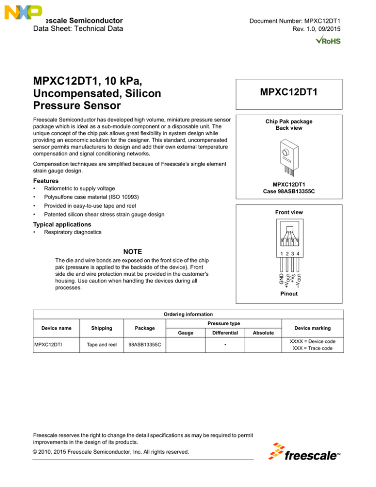
Freescale Semiconductor has developed high volume, miniature pressure sensor
package which is ideal as a sub-module component or a disposable unit. The
unique concept of the chip pak allows great flexibility in system design while
providing an economic solution for the designer. This standard, uncompensated
sensor permits manufacturers to design and add their own external temperature
compensation and signal conditioning networks.
Chip Pak package
Back view
Compensation techniques are simplified because of Freescale’s single element
strain gauge design.
Features
MPXC12DT1
Case 98ASB13355C
•
Ratiometric to supply voltage
•
Polysulfone case material (ISO 10993)
•
Provided in easy-to-use tape and reel
•
Patented silicon shear stress strain gauge design
Front view
Typical applications
Respiratory diagnostics
NOTE
1 2 3 4
The die and wire bonds are exposed on the front side of the chip
pak (pressure is applied to the backside of the device). Front
side die and wire protection must be provided in the customer's
housing. Use caution when handling the devices during all
processes.
GND
+VOUT
+VS
–VOUT
•
Pinout
Ordering information
Pressure type
Device name
Shipping
Package
Device marking
Gauge
MPXC12DTI
Tape and reel
98ASB13355C
Differential
Absolute
•
Freescale reserves the right to change the detail specifications as may be required to permit
improvements in the design of its products.
© 2010, 2015 Freescale Semiconductor, Inc. All rights reserved.
XXXX = Device code
XXX = Trace code
Contents
1
2
3
4
General Description . . . . . . . . . . . . . . . . . . . . . . . . . . . . . . . . . . . . . . . . . . . . . . . . . . . . . . . . . . . . . . . . . . . . . . . . . . . . . .
1.1 Block diagram . . . . . . . . . . . . . . . . . . . . . . . . . . . . . . . . . . . . . . . . . . . . . . . . . . . . . . . . . . . . . . . . . . . . . . . . . . . . . . .
1.2 Pinout . . . . . . . . . . . . . . . . . . . . . . . . . . . . . . . . . . . . . . . . . . . . . . . . . . . . . . . . . . . . . . . . . . . . . . . . . . . . . . . . . . . . .
Mechanical and Electrical Specifications. . . . . . . . . . . . . . . . . . . . . . . . . . . . . . . . . . . . . . . . . . . . . . . . . . . . . . . . . . . . .
2.1 Maximum ratings. . . . . . . . . . . . . . . . . . . . . . . . . . . . . . . . . . . . . . . . . . . . . . . . . . . . . . . . . . . . . . . . . . . . . . . . . . . . .
2.2 Operating characteristics . . . . . . . . . . . . . . . . . . . . . . . . . . . . . . . . . . . . . . . . . . . . . . . . . . . . . . . . . . . . . . . . . . . . . .
Package Dimensions . . . . . . . . . . . . . . . . . . . . . . . . . . . . . . . . . . . . . . . . . . . . . . . . . . . . . . . . . . . . . . . . . . . . . . . . . . . . .
3.1 Package description . . . . . . . . . . . . . . . . . . . . . . . . . . . . . . . . . . . . . . . . . . . . . . . . . . . . . . . . . . . . . . . . . . . . . . . . . .
Revision History . . . . . . . . . . . . . . . . . . . . . . . . . . . . . . . . . . . . . . . . . . . . . . . . . . . . . . . . . . . . . . . . . . . . . . . . . . . . . . . . .
3
3
3
4
4
4
5
5
6
Related Documentation
The MPXC12DT1 device features and operations are described in a variety of reference manuals, user guides, and application
notes. To find the most-current versions of these documents:
1.
Go to the Freescale homepage at:
http://www.freescale.com/
2.
3.
In the Keyword search box at the top of the page, enter the device number MPXC12DT1.
In the Refine Your Result pane on the left, click on the Documentation link.
MPXC12DT1
2
Sensors
Freescale Semiconductor, Inc.
1
General Description
Freescale Semiconductor's biocompatible pressure sensors have been designed for medical usage by combining the
performance of the shear stress pressure sensor design and the use of biomedically approved materials. Materials with a proven
history in medical situations have been chosen to provide a sensor that can be used with confidence in applications, such as
invasive blood pressure monitoring. It can be sterilized using ethylene oxide. The portions of the pressure sensor that are
required to be biomedically approved are the rigid housing and the gel coating. The MPXC12DT1 does not come with gel on the
backside of the device. This enables the customer to customize sensor with gel specific to the intended application space.
The rigid housing is molded from a white, medical grade polysulfone that has passed extensive biological testing including: ISO
10993-5:1999, ISO 10993-10:2002, and ISO 10993-11:1993.
1.1
Block diagram
Figure 1 shows a block diagram of the internal circuitry integrated on a pressure sensor chip.
+VS
Sensing
Element
+VOUT
–VOUT
GND
Figure 1. Block diagram
1.2
Pinout
GND
+VOUT
+VS
–VOUT
1 2 3 4
Figure 2. Device pinout (front view)
Table 1. Pin functions
Pin
Name
Function
1
GND
2
+VOUT
Ground
Output voltage
3
+VS
Voltage supply
4
–VOUT
Output voltage
MPXC12DT1
Sensors
Freescale Semiconductor, Inc.
3
2
Mechanical and Electrical Specifications
2.1
Maximum ratings
Table 2. Maximum ratings(1)
Symbol
Value
Unit
Maximum pressure (backside)
Rating
Pmax
75
kPa
Storage temperature
Tstg
-25 to +85
°C
Operating temperature
TA
+15 to +40
°C
1. Exposure beyond the specified limits may cause permanent damage or degradation to the device.
2.2
Operating characteristics
Table 3. Operating characteristics (VS = 3.0 VDC, TA = 25 °C unless otherwise noted, P1 > P2)
Characteristic
Symbol
Min
Typ
Max
Unit
POP
0
—
10
kPa
Supply voltage
VS
—
3
6
VDC
Supply current
IO
—
6.0
—
mAdc
Full-scale span(3)
VFSS
45
65
80
mV
Offset(4)
VOFF
0
20
35
mV
Sensitivity
Pressure range(1)
(2)
ΔV/ΔP
—
6.5
—
mV/kPa
Linearity
—
0
—
10
%VFSS
Pressure hysteresis (0 to 10 kPa)
—
—
±0.1
—
%VFSS
Temperature hysteresis (+15 °C to +40 °C)
—
—
±0.1
—
%VFSS
Input impedance
Output impedance
Response time
(5)
ZIN
400
—
550
Ω
ZOUT
750
—
1250
Ω
(10% to 90%)
Warm-up(6)
(7)
Offset stability
tR
—
1.0
—
ms
—
—
20
v
ms
—
—
±0.5
—
%VFSS
1. 1.0 kPa (kilo Pascal) equals 0.145 psi.
2. Device is ratiometric within this specified excitation range. Operating the device above the specified excitation range may induce additional
error due to device self-heating.
3. Full-scale span (VFSS) is defined as the algebraic difference between the output voltage at full rated pressure and the output voltage at the
minimum rated pressure.
4. Offset (VOFF) is defined as the output voltage at the minimum rated pressure.
5. Response time is defined as the time for the incremental change in the output to go from 10% to 90% of its final value when subjected to a
specified step change in pressure.
6. Warm-up time is defined as the time required for the product to meet the specified output voltage after the pressure is stabilized.
7. Offset stability is the product's output deviation when subjected to 1000 hours of Pulsed Pressure, Temperature Cycling with Bias Test.
MPXC12DT1
4
Sensors
Freescale Semiconductor, Inc.
3
Package Dimensions
3.1
Package description
This drawing is located at http://cache.freescale.com/files/shared/doc/package_info/98ASB13355C.pdf.
A
M
C
L
F
N
B
1
2 3
V
4
K
DETAIL A
–T–
D1
G
J
H
FRONT VIEW
E
END VIEW
AC
NOTES:
1. DIMENSIONING AND TOLERANCING PER ANSI
3.
Y14.5M, 1982.
2. CONTROLLING DIMENSION: INCH.
4.
F
AA
AB
AD
D2
DETAIL A
BACK VIEW
DIM
A
B
C
D1
D2
E
F
G
H
J
K
L
M
N
V
AA
AB
AC
AD
INCHES
MIN
MAX
0.240
0.260
0.350
0.370
0.140
0.150
0.012
0.020
0.014
0.022
0.088
0.102
0.123
0.128
0.045
0.055
0.037
0.047
0.007
0.011
0.120
0.140
0.095
0.105
0.165
0.175
0.223
0.239
0.105
0.115
0.095
0.107
0.015
0.035
0.120
0.175
0.100
0.115
MILLIMETERS
MIN
MAX
6.10
6.60
8.89
9.40
3.56
3.81
0.30
0.51
0.36
0.56
2.24
2.59
3.12
3.25
1.14
1.40
0.94
1.19
0.18
0.28
3.05
3.56
2.41
2.67
4.19
4.45
5.66
6.07
2.67
2.92
2.41
2.72
0.38
0.89
3.05
4.45
2.54
2.92
Case 98ASB1335C, Chip Pak package
MPXC12DT1
Sensors
Freescale Semiconductor, Inc.
5
4
Revision History
Table 4. Revision history
Revision
number
Revision
date
0
11/2010
• Initial release.
1
08/2015
• Updated format.
Description
MPXC12DT1
6
Sensors
Freescale Semiconductor, Inc.
How to Reach Us:
Information in this document is provided solely to enable system and software
Home Page:
freescale.com
implementers to use Freescale products. There are no express or implied copyright
Web Support:
freescale.com/support
information in this document.
licenses granted hereunder to design or fabricate any integrated circuits based on the
Freescale reserves the right to make changes without further notice to any products
herein. Freescale makes no warranty, representation, or guarantee regarding the
suitability of its products for any particular purpose, nor does Freescale assume any
liability arising out of the application or use of any product or circuit, and specifically
disclaims any and all liability, including without limitation consequential or incidental
damages. “Typical” parameters that may be provided in Freescale data sheets and/or
specifications can and do vary in different applications, and actual performance may
vary over time. All operating parameters, including “typicals,” must be validated for each
customer application by customer’s technical experts. Freescale does not convey any
license under its patent rights nor the rights of others. Freescale sells products pursuant
to standard terms and conditions of sale, which can be found at the following address:
freescale.com/salestermsandconditions.
Freescale and the Freescale logos are trademarks of Freescale Semiconductor, Inc.,
Reg. U.S. Pat. & Tm. Off. All other product or service names are the property of their
respective owners.
© 2010, 2015 Freescale Semiconductor, Inc.
Document Number: MPXC12DT1
Rev. 1.0
09/2015
