Small Signal Averaged Model of DC Choppers for Control Studies
advertisement

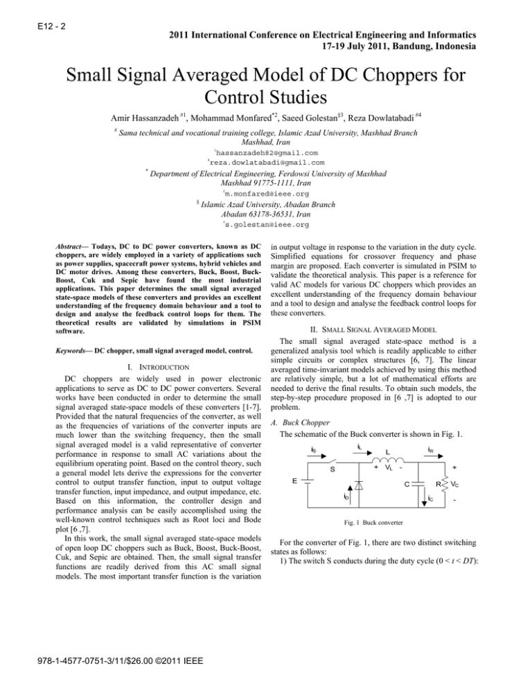
E12 - 2 2011 International Conference on Electrical Engineering and Informatics 17-19 July 2011, Bandung, Indonesia Small Signal Averaged Model of DC Choppers for Control Studies Amir Hassanzadeh #1, Mohammad Monfared*2, Saeed Golestan§3, Reza Dowlatabadi #4 # Sama technical and vocational training college, Islamic Azad University, Mashhad Branch Mashhad, Iran 1 hassanzadeh82@gmail.com reza.dowlatabadi@gmail.com 4 * Department of Electrical Engineering, Ferdowsi University of Mashhad Mashhad 91775-1111, Iran 2 § m.monfared@ieee.org Islamic Azad University, Abadan Branch Abadan 63178-36531, Iran 3 s.golestan@ieee.org Abstract— Todays, DC to DC power converters, known as DC choppers, are widely employed in a variety of applications such as power supplies, spacecraft power systems, hybrid vehicles and DC motor drives. Among these converters, Buck, Boost, BuckBoost, Cuk and Sepic have found the most industrial applications. This paper determines the small signal averaged state-space models of these converters and provides an excellent understanding of the frequency domain behaviour and a tool to design and analyse the feedback control loops for them. The theoretical results are validated by simulations in PSIM software. Keywords— DC chopper, small signal averaged model, control. I. INTRODUCTION DC choppers are widely used in power electronic applications to serve as DC to DC power converters. Several works have been conducted in order to determine the small signal averaged state-space models of these converters [1-7]. Provided that the natural frequencies of the converter, as well as the frequencies of variations of the converter inputs are much lower than the switching frequency, then the small signal averaged model is a valid representative of converter performance in response to small AC variations about the equilibrium operating point. Based on the control theory, such a general model lets derive the expressions for the converter control to output transfer function, input to output voltage transfer function, input impedance, and output impedance, etc. Based on this information, the controller design and performance analysis can be easily accomplished using the well-known control techniques such as Root loci and Bode plot [6 ,7]. In this work, the small signal averaged state-space models of open loop DC choppers such as Buck, Boost, Buck-Boost, Cuk, and Sepic are obtained. Then, the small signal transfer functions are readily derived from this AC small signal models. The most important transfer function is the variation 978-1-4577-0751-3/11/$26.00 ©2011 IEEE in output voltage in response to the variation in the duty cycle. Simplified equations for crossover frequency and phase margin are proposed. Each converter is simulated in PSIM to validate the theoretical analysis. This paper is a reference for valid AC models for various DC choppers which provides an excellent understanding of the frequency domain behaviour and a tool to design and analyse the feedback control loops for these converters. II. SMALL SIGNAL AVERAGED MODEL The small signal averaged state-space method is a generalized analysis tool which is readily applicable to either simple circuits or complex structures [6, 7]. The linear averaged time-invariant models achieved by using this method are relatively simple, but a lot of mathematical efforts are needed to derive the final results. To obtain such models, the step-by-step procedure proposed in [6 ,7] is adopted to our problem. A. Buck Chopper The schematic of the Buck converter is shown in Fig. 1. Fig. 1 Buck converter For the converter of Fig. 1, there are two distinct switching states as follows: 1) The switch S conducts during the duty cycle (0 < t < DT): PM arctan( 4 LER 2 C 2 L2 ) 2(1 E )CR 2 L (7) B. Boost Chopper The modelling procedure is the same as the steps followed for the Buck chopper. So, as a matter of simplicity, just the final results are reported. The Boost converter is shown in Fig. 3. The small signal averaged state-space model is as follows: dvˆc 1 D ' IL dt C vˆc 0 RC C (8) dˆ 1 eˆ Vc iˆL diˆL D ' 0 L dt L L And the small signal transfer function of the output voltage variation due to the duty cycle change is: I D' Vc L s vˆc ( s ) C LC (9) s D '2 dˆ ( s ) 2 s RC LC where D΄ = 1 – D. Comparing the Bode plots of Fig. 4, shows that the analytical results are in good agreement with the experiments. 20 Fig. 3 Boost converter 0 -20 40 3 30 4 10 10 0 pahse (deg) The gain margin is infinite and the simplified relations for the crossover frequency, ω0, and the phase margin, PM, are as bellow: E 1 (6) 0 2 2 LC 2 R C Mag (dB) Mag (dB) vc dvc 1 dt C (iL R ) (1) diL 1 (e v ) c dt L where D and T are the duty cycle and the switching period, respectively. 2) The switch is off during the rest of the switching period (DT < t < T): vC dvc 1 dt C (iL R ) (2) diL 1 (v ) C dt L Based on equations (1) and (2), the small signal averaged state-space model is obtained as bellow, in which the variables with a hat are small AC variations about the equilibrium operating point: dvˆc 1 1 0 dt vˆc 0 RC C D eˆ E dˆ (3) diˆL 1 iˆL 0 L L dt L By applying the Laplace transform to (3) the following small signal transfer function of the output voltage variation due to the duty cycle change is obtained: E vˆc ( s ) LC (4) dˆ ( s ) s 2 s 1 RC LC The Bode plots of the transfer function of equation (4) and the experimental circuit simulated in PSIM are compared in Fig. 2 which confirms the validity of the obtained analytical results. 20 10 0 -50 3 4 10 10 -100 3 pahse (deg) -150 4 10 10 Frequency (Hz) Fig. 2 Bode plot of control to output (Buck converter) (-): analytical (--): experimental 300 200 100 3 This converter has two poles as: 1 1 1 P1,2 2 RC (2 RC ) 2 LC 4 10 10 Frequency (Hz) (5) Fig. 4 Bode plot of control to output (Boost converter) (-): analytical (--): experimental This converter has two poles and a right half-plane zero as: C. Buck-Boost Chopper The Buck-Boost converter is shown in Fig. 5. The small signal averaged state-space model and the transfer function of control to output are as equations (13) and (14). dvˆc 1 D ' IL dt C vˆc 0 RC C (13) dˆ D eˆ Vc E iˆL diˆL D ' 0 L dt L L I D' L s (Vc E ) vˆc ( s ) C LC (14) s D '2 dˆ ( s ) 2 s RC LC The analytical Bode plot is validated by the experimental results in Fig. 6. Obviously, the frequency domain performance is similar to the Boost converter. Fig. 5 Buck-Boost converter Similar to the Boost converter, this converter has two poles and a right half-plane zero as: D '(Vc E ) 1 1 D '2 , Z (15) 2 2 RC LC LI L (2 RC ) The simplified equations for the crossover frequency and the phase margin are: I (16) 0 L C L IL LI L 2 R ) arctan PM arctan( (17) 2 2 CD '(Vc E ) LI L CD ' P1,2 40 Mag (dB) 30 20 10 0 3 4 10 pahse (deg) D 'Vc 1 1 D '2 P1,2 , Z (10) 2 2 RC LC LI L (2 RC ) The simplified equations for the crossover frequency and the phase margin are: I (11) 0 L C L IL LI L 2 R ) arctan PM arctan( (12) 2 2 ' CD 'Vc LI C D L 10 300 200 100 3 4 10 10 Frequency (Hz) Fig. 6 Bode plot of control to output (Buck-Boost converter) (-): analytical (--): experimental D. Cuk Chopper The Cuk converter is shown in Fig. 7. Fig. 7 Cuk converter Equations (18) and (19) are the small signal averaged statespace model and the transfer function of control to output, respectively. The Bode plots are depicted in Fig. 8. Experimental waveforms agree with the analytical results. The Cuk converter has four left half-plane poles and two right half-plane zeros. D' D dvˆc1 0 0 IL1 IL2 dt C1 C1 C 0 1 ˆ v c1 1 1 0 0 dvˆc2 0 0 vˆ dt RC2 C2 c2 1 eˆ Vc1 d̂ (18) ˆ ˆ D ' di i L1 L1 0 0 0 L L 1 1 dt L iˆL2 0 V 1 c1 1 diˆL2 D L 0 0 2 dt L2 L2 vˆc 2 (s) dˆ (s) Vc1 DL1 C1LV 1 c1 2 D'2 s D'2 I L1 I L2 s D ' D2 2 L2 L1D2 C1C2 L1 L2 4 C1L1 L2 3 C1 L1 D'2 s RD'2 s D'2 C2 (L2 L1 D' 2 ) s R RD'2 s 1 (19) These converters must first store the energy in the inductor during a certain time before dumping it into the output capacitor during the rest of the switching period. If the duty cycle quickly changes in response to a perturbation, the inductor naturally limits the current slew rate and the output voltage drops. The presence of right half-plane zeros means a serious limit on the available loop bandwidth. Mag (dB) 40 20 0 3 4 10 10 III. CONCLUSIONS Thanks to their advantages, Buck, Boost, Buck-Boost, Cuk and Sepic choppers have found a lot of industrial applications. In this paper, the small signal averaged state-space models of these converters are obtained which provide an excellent understanding of the frequency domain behaviour and a tool to design and analyse the feedback control loops for these converters. The theoretical results are validated by simulations in PSIM software. pahse (deg) 300 200 100 0 -100 3 4 10 10 Frequency (Hz) Fig. 8 Bode plot of control to output (Cuk converter) (-): analytical (--): experimental 50 40 Mag (dB) E. Sepic Chopper The Sepic converter is shown in Fig. 9. 30 20 10 0 3 4 10 10 Fig. 9 Sepic converter pahse (deg) 600 The small signal averaged state-space model and the transfer function of output to control are as equations (20) and (21) and the Bode plot are depicted in Fig. 10. D' D IL1 IL2 dvˆc1 0 0 C dt C1 C1 1 0 vˆ dvˆc2 0 1 D' D' c1 0 IL1 IL2 dt C2 ˆ RC2 C2 C2 vˆc2 1 eˆ d (20) iˆL1 Vc1 Vc2 diˆL1 D' D' 0 0 L 1 dt L L1 iˆL2 0 L1 1 D' Vc1 Vc2 diˆL2 D 0 0 dt L L2 2 L2 The Sepic chopper has four left half-plane poles and three right half-plane zeros. The apparent feature for all converters under the study is the resonance and Boost, Buck-Boost, Cuk and Sepic choppers, as indirect energy transfer converters, suffer from the presence of right half-plane zeros. The physical origin of the right half-plane zero is the indirect energy transfer in boost operation. 400 200 3 4 10 10 Frequency (Hz) Fig. 10 Bode plot of control to output (Sepic converter) (-): analytical (--): experimental REFERENCES [1] [2] [3] [4] [5] [6] [7] L. K. Wong, and T. K. Man, “Small signal modeling of open-loop SEPIC converters,” IET Power Electron., vol. 3, lss. 6, pp. 858–868, May 2010. J. Xu, “An analytical technique for the analysis of switching DC-DC converters,” in Proc. ISCAS’91, 1991, pp. 1212-1215. G. N. Love, and A. R. Wood, “Small signal model of a power electronic converter,” in Proc. IPEC’07, 2007, pp. 636-642. J. Lee, “Analysis of small-signal model of a PWM DC-DC Buck-Boost converter in CCM,” M. Eng. thesis, Wright State University, Dayton, OH, 2005. F. L. Luo, and H. Ye, “small signal analysis of energy factor and mathematical modeling for power DC–DC converters,” IEEE Trans. Power Electron., vol. 22, no. 1, pp. 69-79, 2007. R. W. Erickson, Fundamentals of Power Electronics, 1st ed., New York: Chapman and Hall, 1997. J. G. Kassakian, M. F. Schlecht, and G. C. Verghese, Principles of Power Electronics, 1st ed., Reading, Massachusetts: Addison-Wesley, 1991. RC1 L1 L2 I L1 I L 2 s 3 D ' RC1 (Vc1 Vc 2 ) L1 L2 s 2 RDL1 I L1 I L 2 s (2 DD '2 D '3 D ' D 2 ) R Vc1 Vc 2 vˆc 2 ( s ) dˆ ( s ) C1C2 L1 L2 Rs 4 C1 L1 L2 s 3 R L1 (C2 D 2 C1 D '2 ) L2 (C1 C2 ) D '2 s 2 ( D 2 L1 D '2 L2 ) s R ( D '4 2 DD '3 D 2 D '2 ) (21)


