ANALOG IP BLOCK
LVDS_TX - CMOS LVDS Transmitter
DATA SHEET
PROCESS
DESCRIPTION
C35B3 (0.35um)
The LVDS_TX is a differential line driver designed for
applications requiring high data rates. The device supports
data rates up to 1Gb/s (500MHz).
The LVDS_TX accepts CMOS input levels and translates them
to low voltage (350mV) differential output signals, which
provides low EMI even at high frequencies.
FEATURES
LVDS_TX area: 0.184mm2,
LVDS_TX size: x = 533µm y = 345.7µm
TXBIAS area: 0.08mm2,
TXBIAS size: x = 332.4µm y = 239.3µm
3.3V ±10% supply voltage
±350mV differential signaling
1Gb/s maximum transmission speed
800ps maximum propagation delay
Power dissipation 33mW at 3.3V, static, without
TXBIAS
Junction temperature –40 - 125°C
Compatible with IEEE 1596.3 SCI LVDS standard
Internal 100Ω termination resistor
High capacitive loads driving capability:
10pF @ 1Gb/s
Power down mode
Revision D, 08.01.2004
With the companion line receiver (LVDS_RX ) it provides a new
alternative to high power pseudo-ECL devices for high speed
applications.
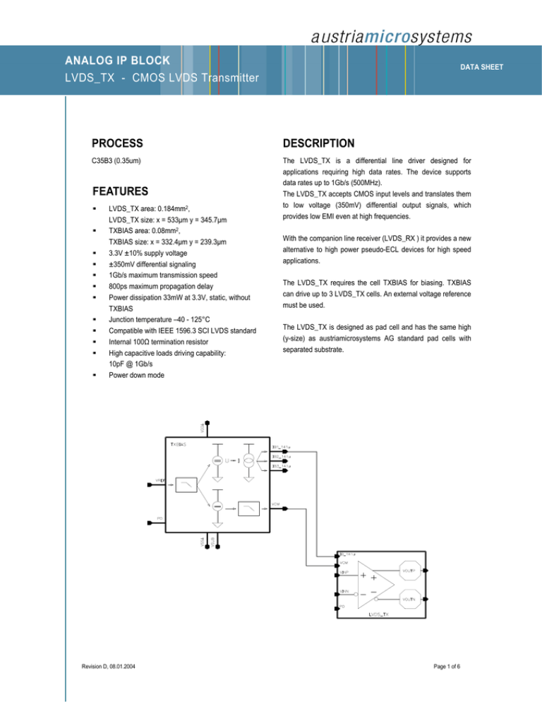
The LVDS_TX requires the cell TXBIAS for biasing. TXBIAS
can drive up to 3 LVDS_TX cells. An external voltage reference
must be used.
The LVDS_TX is designed as pad cell and has the same high
(y-size) as austriamicrosystems AG standard pad cells with
separated substrate.
Page 1 of 6
Datasheet: LVDS_TX - C35
TECHNICAL DATA FOR LVDS_TX
(Tjunction = −40 to 125°C, VDDA = 3.0V to 3.6V, VSSA = VSUB = 0V, VREF = 1.25V, PD = low, receiver input termination resistance
RL = 100Ω, unless otherwise specified)
DC CHARACTERISTICS
Symbol
VOD
Parameter
Differential Output Swing
Conditions
Min
250
Typ
350
Max
450
Units
mV
1.11
1.25
1.37
V
1.425
1.075
1.60
0.88
V
V
V
V
Max
Unit
ps
ps
ps
VOD = |VOUTP – VOUTN|
VOCM
VOH
VOL
VIH
VIL
Common Mode Output Voltage
VOCM = (VOUTP + VOUTN) / 2
Output Voltage High
Output Voltage Low
Input Voltage High
Input Voltage Low
CMOS levels
AC CHARACTERISTICS
Symbol
tPLHD
tPHLD
tSKD1
Parameter
Different. Propagation Delay Low to High
Different. Propagation Delay High to Low
tSKD2
tTLHD
tTHLD
tPZH
tPZL
Cload
Cin
fMAX
TXS
Differential Channel to Channel Skew
Differential Output Rise Time
Differential Output Fall Time
Power Up Time High-Z to High
Power Up Time High-Z to Low
Load Capacitance
Input Capacitance
Maximum Operating Frequency 4)
Transmission Rate
Differential Pulse Skew |tPLHD – tPHLD|
2)
Conditions
Cload = 10pF 1)
Cload = 10pF 1)
Cload = 10pF @1Gb/s1)
Min
Cload = 10pF @1Gb/s1)
Cload = 10pF 1) 3)
Cload = 10pF 1) 3)
Cload = 10pF
Cload = 10pF
@1Gb/s
Typ
400
400
70
80
550
550
300
300
500
500
14
2
500
1000
ps
ps
ps
ns
ns
pF
pF
MHz
Mb/s
Typ
16
Max
25
Unit
mA
8
12
mA
10
16
15
25
mA
mA
33
52.8
10
54
90
36
µA
mW
mW
µW
1
POWER REQUIREMENTS
Symbol
IOS
Parameter
Output Short Circuit Current
IOSD
Differential Output Short Circuit Current
ICCDC
ICCAC
DC Current Consumption
AC Current Consumption
ICCPD
Pdiss_DC
Pdiss_AC
Pdiss_PD
Power Down Current Consumption 5)
DC Power Consumption
AC Power Consumption
Power Consumption in Power Down Mode
Conditions
Outputs shorted to
VSSA
VOUTP and VOUTN
shorted, VOD = 0V
No TXBIAS
Cload = 10pF @1Gb/s,
no TXBIAS
PD = high, no TXBIAS
No TXBIAS
No TXBIAS
PD = high, no TXBIAS
Min
1)
Including the package: SOIC28, pins 5–10 or 19–24 for VOUTP and VOUTN
tSKD1 is the magnitude difference in differential propagation delay time between the positive going edge and the negative going edge of the
same channel
3) Specified at 20% and 80% of the output voltage (IEEE 1596.3 SCI LVDS standard)
4) fMAX generator input conditions: tr = tf < 500ps, 50% duty cycle, output criteria: VOD > 250mV
2)
5)
Static input signals: VINP = VDDA, VINN = VSSA
Revision D, 08.01.2004
Page 2 of 6
Datasheet: LVDS_TX - C35
TECHNICAL DATA FOR TXBIAS
(Tjunction = −40 to 125°C, VDDA = 3.0V to 3.6V, VSSA = VSUB = 0V, PD = low, unless otherwise specified)
POWER REQUIREMENTS
Symbol
ICC
Parameter
Current Consumption
ICCPD
Power Down Current Consumption
Pdiss
Power Consumption
Pdiss_PD
Power Consumption in Power Down Mode
Conditions
Min
Typ
0.5
1.65
PD = high
Max
1
Unit
mA
200
nA
3.3
mW
720
nW
Max
1.3
Unit
V
EXTERNAL REFERENCE CHARACTERISTICS
Symbol
VREF
Parameter
External Reference Voltage
Conditions
Min
1.2
Typ
1.25
AC WAVEFORMS FOR LVDS_TX
VINN
VIH = 3V
1.5V
1.5V
VINP
VIL = 0V
tPLHD
tPHLD
VOUTN
VOH = 1.425V
1.25 V
1.25 V
VOUTP
VOL = 1.075V
+VOD = +350mV
80%
VOUTP - VOUTN
80%
0V
0V
20%
20%
-VOD = -350mV
tTLHD
Revision D, 08.01.2004
tTHLD
Page 3 of 6
Datasheet: LVDS_TX - C35
TYPICAL PERFORMANCE CURVES
1,50
1,10
RL
= 100Ω
1,46
1,44
1,42
= 100Ω
Tjunc = 25°C
1,06
1,04
1,02
1,40
1,00
3,0
3,1
3,2
3,3
3,4
3,5
3,6
3,1
3,2
3,4
3,5
Output Voltage High vs. Power Supply Voltage
Output Voltage Low vs. Power Supply Voltage
IOSD Differential Output Short Circuit Current [mA]
350
RL
= 100Ω
Tjunc = 25°C
3,6
8,0
7,8
VOD
= 0V
Tjunc = 25°C
7,6
7,4
7,2
7,0
6,8
6,6
250
3,0
3,1
3,2
3,3
3,4
3,5
3
3,6
3,1
3,2
3,3
3,4
3,5
3,6
VDD Power Supply Voltage [V]
VDD Power Supply Voltage [V]
Differential Output Voltage vs. Power Supply
Differential Output Short Circuit Current vs. Power Supply
450
16,0
15,0
VDDA = 3.3V
Tjunc = 25°C
400
ICC Current Consumption [mA]
VOD Differential Output Voltage [mV]
3,3
VDD Power Supply Voltage [V]
400
300
3,0
VDD Power Supply Voltage [V]
450
VOD Differential Output Voltage [mV]
RL
1,08
Tjunc = 25°C
VOL Output Voltage Low [V]
VOH Output Voltage High [V]
1,48
350
300
VDDA = 3.3V
14,0
13,0
RL
= 100Ω
CL
= 10pF
Tjunc = 25°C
12,0
11,0
10,0
9,0
250
8,0
80
85
90
95
100
105
110
115
RL Load Resistor [Ohm]
Differential Output Voltage vs. Load Resistor
Revision D, 08.01.2004
120
0,1
1,0
10,0
100,0
Frequency [MHz]
Current Consumption vs. Frequency
Page 4 of 6
1000,0
Datasheet: LVDS_TX - C35
SYMBOL OF LVDS_TX
PIN LIST OF LVDS_TX
PD
Low
VINP
High
VINN
Low
VOUTP
VOH
VOUTN
VOL
Low
Low
High
VOL
VOH
High
High
Low
High-Z
High-Z
High
Low
High
High-Z
High-Z
SYMBOL OF TXBIAS
Pin
IB_141u
Description
Bias Current
Type
Analog
VCM
Common Mode Voltage
Analog
VINP
Positive Input
Digital
VINN
Negative Input
Digital
PD
Power Down
Digital
VOUTP
Positive LVDS Output
Analog
VOUTN
Negative LVDS Output
Analog
The LVDS_TX is designed as a pad cell and so there are no
supply pins shown on the symbol. The cell is compatible to the
austriamicrosystems AG power bus with additional substrate bus.
PIN LIST OF TXBIAS
PD
Low
VCM
VREF
IBx_141u
141uA
High
Low
High-Z
Pin
VDDA
Description
Positive Supply
Type
Supply
VSSA
Negative Supply
Supply
VSUB
Substrate
Supply
IB1_141u
IB2_141u
IB3_141u
Bias Current
Analog
VCM
Common Mode Voltage
Analog
PD
Power Down
Digital
VREF
External Reference Voltage
Analog
THEORY OF OPERATION
The LVDS_TX is a differential line driver with a low voltage output
swing. The output voltage levels are generated with current
sources applied to the internal termination resistors. An output
voltage change is achieved by switching the internal current
sources. The 100Ω differential termination is provided both at the
transmitter and receiver end, therefore only 50Ω transmission
lines are needed (no external termination resistor is necessary).
Revision D, 08.01.2004
Page 5 of 6
Datasheet: LVDS_TX - C35
APPLICATION
High Speed Backplane Driver
Complementary Clock Drivers
Level Translator
System Interconnects
ATM Applications
SDH Applications
High-Resolution Imaging Applications
Laser Printers
Digital Copiers
TYPICAL APPLICATION
1)2)3)4)5)
chip internal
external
SNAP BACK 3)
VREF
4)
VREF (ext. reference)
1nF
180pF
VSSA
CLK
complementary
CMOS signals
(from digital core)
50Ω transmission lines
CLK_N
to receiver
SDATA
complementary
CMOS signals
(from digital core)
50Ω transmission lines
SDATA_N
to receiver
SYNC
complementary
CMOS signals
(from digital core)
50Ω transmission lines
SYNC_N
to receiver
5)
2)
5)
5)
VSSA 1)
5)
4)
5)
4)
VDDA 1)
VDDA
1 µF
100pF
22pF
VSSA
SNAP BACK 3)
1)
2)
3)
4)
5)
The two supply pads can be bonded to one package pin (double bonding)
The substrate pin must be connected on PCB level to VSSA
The LVDS part of the chip has to be separated from the rest of the chip using snap back devices (cell PWRCUT_DIG_P_SNAP_SNAP_3B)
The cells VDD3R1_3B, VDD3R2O_3B and APRIO200P_3B_R2O are not in the standard library, they are part of the IP-block
The supply pads are connected to the LVDS_TX via the periphery power supply bus
Revision D, 08.01.2004
Page 6 of 6
Datasheet: LVDS_TX - C35
Contact
Copyright
austriamicrosystems AG
A 8141 Schloss Premstätten, Austria
T. +43 (0) 3136 500 5333
F. +43 (0) 3136 500 5755
support@austriamicrosystems.com
Copyright © 2002 austriamicrosystems. Trademarks registered ®.
All rights reserved. The material herein may not be reproduced,
adapted, merged, translated, stored, or used without the prior
written consent of the copyright owner. To the best of its
knowledge, austriamicrosystems asserts that the information
contained in this publication is accurate and correct.
Revision D, 08.01.2004
Page 7 of 6


