AVR1301: Using the XMEGA DAC
Features
•
•
•
•
•
•
8-bit
Microcontrollers
12 bit resolution
Up to 1 M conversions per second
Continuous drive or sample-and-hold output
Built-in offset and gain calibration
High drive capabilities
Driver source code included
Application Note
1 Introduction
The XMEGA™ DAC module is a high-performance Digital-to-Analog converter
capable of conversion rates up to 1 M conversions per second with a resolution of
12 bits. High output driving capabilities, dual sample-and-hold outputs and optional
routing of DAC output to on-board comparator or Analog-to-Digital converter (ADC)
make this a flexible module suitable for a huge range of applications, such as
stereo sound output, high-speed signal generation, calibration and signal
compensation.
This application note describes the basic functionality of the XMEGA DAC with
code examples to get up and running quickly. A driver interface written in C is
included as well.
Advanced use, such as Direct Memory Access (DMA) and the XMEGA Event
System, is outside the scope of this application note. Please refer to the device
datasheets and other relevant application notes for details.
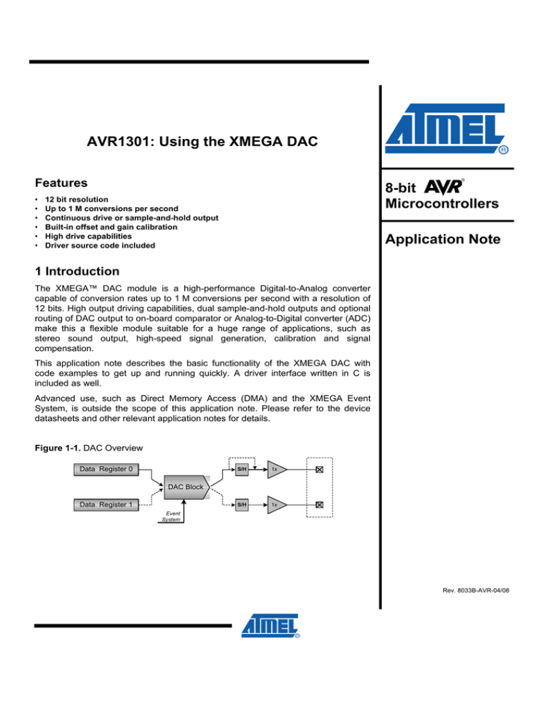
Figure 1-1. DAC Overview
Data Register 0
S/H
1x
S/H
1x
DAC Block
Data Register 1
Event
System
Rev. 8033B-AVR-04/08
2 Module Overview
This section provides an overview of the basic configuration options and functionality
of the DAC. Section 3 then walks you through the basic steps to get up and running,
with register descriptions and configuration details.
2.1 Conversion Triggers
A DAC conversion can be triggered either by (1) the data registers being written to or
(2) from an incoming event from the XMEGA Event System.
When triggered by data write operations, the conversion starts when the high byte
register is updated.
When the Event System is used, the conversion starts when an event arrives, not
when the data registers are updated. This means that the data registers can be
updated several times without triggering any conversion. When the event arrives, the
current value of the data registers are used in the conversion.
Even if software that manually writes to the data registers could achieve fairly good
timing, it is recommended to use a timer base together with events and DMA
transfers for applications that require precise timing. However, for applications that do
not have strict timing requirements or use static output values, it is not necessary to
utilize these advanced features.
Trigger mode is configured with the Trigger Mode bits (CHnTRIG) in Control Register
B (CTRLB). Note that trigger mode can be individually configured for the two
channels. For instance, channel 0 can be triggered on data write while channel 1
uses events.
2.2 Single and Dual Channel Operation
The DAC module contains two data channels with corresponding data registers, but
only one conversion block. The user can choose between using channel 0 as a
continuous-drive output or both channels as two Sample/Hold outputs.
The channel operation mode is configured with the Channel Select bitfield (CHSEL) in
Control Register B (CTRLB).
2.2.1 Single Channel Operation
In single channel operation, the DAC conversion block is always connected to the
data registers and output driver stage of channel 0. Hence the concept continuousdrive output.
Figure 2-1 below shows the DAC in single channel operation mode. Note that the
Sample/Hold stage is bypassed.
2
AVR1301
8033B-AVR-04/08
AVR1301
Figure 2-1. Single Channel Operation
Data Register 0
DAC Block
1x
Event
System
2.2.2 Dual Channel Operation
In dual channel operation, the DAC conversion block is alternately used to convert
values for channel 0 and 1. Sample/Hold blocks are used to keep the output values
between conversions. To be able to maintain a stable output value on the two
outputs, the channels need to be refreshed regularly. Please consult the Electrical
Characteristics section of the datasheet for details on minimum refresh rate. Note that
a higher refresh rate causes higher power consumption. Detail on power consumption
versus conversion rate is also found in the datasheet.
The event system could be used to maintain the required refresh rate, but in most
cases, the event system is used to generate the sample rate instead. If the sample
rate is slower than the refresh rate, the DAC module has an internal refresh interval
generator as well. The automatic refresh interval is configured with the Refresh
Timing Control bitfield (REFRESH) in the Timing Control register (TIMCTRL).
Note that manual conversions or event triggering does not affect the refresh interval.
This means that the channels will be refreshed at constant intervals even if extra
conversions are done in between, caused by for instance a manual update of a data
register. Figure 2-2 below shows an example. The sample interval is covered in the
Section 2.2.3.
Figure 2-2. Channel refresh and conversion request
Sample Interval
Refresh Interval
Channel 0
Convert&Sample
Channel 1
Convert&Sample
Refresh interval
Channel 0
update or event
Channel 1
update or event
1
2
3
4
5
6
1) A refresh interval starts and a conversion and sampling of channel 0 follows.
After one sample interval, channel 1 is converted and sampled.
2) A conversion request (register update or event) for channel 0 triggers a
conversion and sampling of channel 0 only, even if we are in the middle of
one refresh interval.
3) Another refresh interval starts, similar to 1).
3
8033B-AVR-04/08
4) A conversion request (register update or event) for channel 1 triggers a
conversion and sampling of channel 1 only, even if both channels were just
refreshed.
5) Another refresh interval starts, similar to 1). Note that the conversion request
for channel 0 is delayed until 6).
6) The delayed conversion request from 5) triggers another conversion and
sampling of channel 0 immediately after finishing channel 1.
Note that if the arrival rate of conversion requests approaches the refresh rate, the
conversion timing might become imprecise, as an ordinary refresh could be in
progress when the conversion request arrives. A request that arrive in the middle of a
refresh is delayed until both channels have been refreshed. If more than one request
arrives for a channel before the first one is served, the extra requests will be ignored.
If this is a problem for the application in question, a solution is to disable the
automatic refresh interval and instead ensure that the data arrives at a high enough
rate. Note that it is not possible to turn of automatic refresh for one channel only.
2.2.3 Sample Interval
When using dual channel operation, there is a certain minimum time delay required
from conversion of channel 0 starts until channel 1 can start. This is due to a finite
settling time of the DAC conversion block output. This delay is minimum 1 µs, which
limits the sample rate to maximum 1 MHz.
The sample interval is configured with the Channel Separation Control bitfield
(CHSEP) in the Timing Control register (TIMCTRL).
2.3 Left and Right Adjusted Values
The 12-bit input value to the DAC is contained in two 8-bit registers, referred to as the
high and low registers. By default, the 12-bit value is distributed with the 8 LSB in the
low register and 4 MSB in the high register. This distribution is convenient when the
application stores 12-bit DAC values as 16-bit integers, e.g. unsigned short int.
However, some applications find it useful to work with left-adjusted data, e.g. 16-bit
values where the 4 LSB is treated as a fractional part. Another alternative is that the
application stores DAC values in 8-bit variables, e.g. unsigned char, and thus
leaves the 4 LSB of the 12-bit DAC value equal to zero.
The XMEGA DAC module can be configured to accept left adjusted values by setting
the Left-adjust Value bit (LEFTADJ) in Control Register C (CTRLC). Figure 2-3 shows
the difference between right and left adjusted values in the DAC value registers.
4
AVR1301
8033B-AVR-04/08
AVR1301
Figure 2-3. Left and Right Adjusted Values
High Register
Low Register
MSB
LSB
Right-adjusted value (default)
High Register
MSB
Low Register
LSB
Left-adjusted value
2.4 Voltage References
The application can choose between the following voltage references for conversions:
• Bandgap Reference (1.1V)
• Analog voltage supply (VDD)
• External reference (VREF+)
Note that the external reference pin VREF+ is shared with the ADC module. The
voltage reference is select with the Reference bitfield (REFSEL) in Control Register C
(CTRLB).
2.5 Driving Strength
Regardless of operation mode, the DAC outputs are capable of driving external
resistive loads of 1 kΩ or capacitive loads of 100 pF. Please refer to the module
datasheet for detailed characteristics.
2.6 Calibration
To achieve optimal accuracy for the DAC output, the built-in calibration capabilities
allows fine-tuning of process related offset and gain errors. Two registers, Gain
Calibration (GAINCAL) and Offset Calibration (OFFSETCAL), are used for this
purpose. Both calibration register use 7 bits, where the MSB (bit 6) determines the
direction of the calibration and the 6 LSBs (bit 5..0) determine the calibration
amplitude.
When calibrating the DAC, you need to measure the output somehow. For this
purpose, the DAC can be internally connected to one of the ADC channels (with a
properly calibration ADC) or some external equipment. Using the XMEGA ADC
module enables fully automatic DAC calibration, while using external equipment might
give even higher accuracy if required. For more information on the ADC module,
please refer to the device datasheet or the application note “AVR1000: Getting
Started with the XMEGA ADC”.
When calibrating, first tune the offset value until a value of 0x800 gives exactly half
the reference voltage. Then tune the gain value until a value of 0xFFF gives exactly
5
8033B-AVR-04/08
full reference voltage. Note that it is not possible to tune the gain value using 0x000,
as the conversion block is not able to reach down to 0V.
The calibration is not affected by single or dual channel modes, as the same DAC
block is used for both modes.
A flowchart for the calibration process is shown in Figure 2-4 below.
Figure 2-4. Calibration of DAC using the ADC
Configure ADC channel to
measure internal DAC output
Set DAC value to 0xFFF
Set DAC value to 0x800
Read ADC and determine
gain tuning direction
Read ADC and determine
offset tuning direction
Tune gain value by linear or
binary search
Tune offset value by linear or
binary search
Store calibration values in
EEPROM if required
Gain calibration
Offset calibration
DAC Calibration
END
3 Getting Started
This section walks you through the basic steps for getting up and running with simple
conversions and experimenting with different operating modes. The necessary
registers are described along with relevant bit settings.
3.1 Single Channel Operation
Task: Set static value on DAC channel 0 in single channel operation using analog
supply voltage as conversion reference.
• Set the Channel Select bitfield (CHSEL) in Control Register B (CTRLB) equal to
0x00 to select single channel operation.
• Clear the Event Trig Enable bit for channel 0 (CH0TRIG) in Control Register B
(CTRLB) to trigger conversions when data is written, instead of trigging on
incoming events.
• Set the Reference Selection bitfield (REFSEL) in Control Register C (CTRLC) equal
to 0x01 to use analog supply voltage as conversion reference.
• Set the Channel 0 Enable bit (CH0EN) in Control Register A (CTRLA) to enable
DAC output 0.
• Set the Enable bit (ENABLE) in Control Register A (CTRLA) to enable the DAC
module itself.
• Write a 12-bit right adjusted value to Channel 0 Data register (CH0DATA) to trigger
a conversion. Note that the low byte must be written first.
Note that the data registers are right adjusted by default.
6
AVR1301
8033B-AVR-04/08
AVR1301
3.2 Dual Channel Operation
Task: Set static value on both DAC channels in dual channel operation using analog
supply voltage as conversion reference.
• Set the Channel Select bitfield (CHSEL) in Control Register B (CTRLB) equal to
0x02 to select dual channel operation.
• Clear the Event Trig Enable bit for channel 0 and 1 (CH0TRIG and CH1TRIG) in
Control Register B (CTRLB) to trigger conversions when data is written, instead of
trigging on incoming events.
• Set the Reference Selection bitfield (REFSEL) in Control Register C (CTRLC) equal
to 0x01 to use analog supply voltage as conversion reference.
• Set the Channel 0 Enable and Channel 1 Enable bits (CH0EN and CH1EN) in
Control Register A (CTRLA) to enable both DAC outputs.
• Set the Channel Separation bitfield (CHSEP) in the Timing Control register
(TIMCTRL) equal to 0x04 to use 16 clock cycles for the sample interval, which
means 2 µs with a peripheral clock of 8 MHz.
• Set the Refresh Timing bitfield (REFRESH) in the Timing Control register (TIMCTRL)
equal to 0x06 to use 128 clock cycles for the refresh interval, which means 16 µs
with a peripheral clock of 8 MHz.
• Set the Enable bit (ENABLE) in Control Register A (CTRLA) to enable the DAC
module itself.
• Write 12-bit right adjusted values to the channel data register to trigger
conversions. The outputs will be refreshed every 16 µs when no data is written to
the data registers.
4 Advanced Features
This section introduces more advanced features and possibilities with the DAC. Indepth treatment is outside the scope of this application note and the user is advised
to study the device datasheet and relevant application notes.
Note that the DAC module does not use interrupts.
4.1 DMA Controller
Instead of using polling or timed code to write data and start conversions, it is
possible to use the XMEGA DMA Controller to move data to the conversion registers
from memory buffers or other peripheral modules. This moving of data is done without
CPU intervention, and leaves the CPU ready for other tasks. Note that it is
recommended to use the Event System as conversion trigger source when using
DMA to achieve accurate conversion timing.
For more information, please refer to the device datasheet or the application note
“AVR1304: Getting Started with the XMEGA DMA Controller”.
4.2 Event System
To improve conversion timing and further offload work from the CPU, the DAC is
connected to the XMEGA Event System. This makes it possible to use incoming
events to trigger data conversions.
For more information, please refer to the device datasheet or the application note
“AVR1303: Getting Started with the XMEGA Event System”.
7
8033B-AVR-04/08
5 Driver Implementation
This application note includes a source code package with a basic DAC driver
implemented in C. It is written for the IAR Embedded Workbench® compiler, but it is
also compatible with AVR-GCC.
Note that this DAC driver is not intended for use with high-performance code. It is
designed as a library to get started with the DAC. For timing and code space critical
application development, you should access the DAC registers directly. Please refer
to the driver source code and device datasheet for more details.
5.1 Files
The source code package consists of three files:
• dac_driver.c – DAC driver source file
• dac_driver.h – DAC driver header file
• main.c – Example code using the driver
Note that the driver and example code does not include support for DMA data transfer
or the XMEGA Event System.
For a complete overview of the available driver interface functions and their use,
please refer to the source code documentation.
5.2 Doxygen Documentation
All source code is prepared for automatic documentation generation using Doxygen.
Doxygen is a tool for generating documentation from source code by analyzing the
source code and using special keywords. For more details about Doxygen please visit
http://www.doxygen.org. Precompiled Doxygen documentation is also supplied with
the source code accompanying this application note, available from the readme.html
file in the source code folder.
8
AVR1301
8033B-AVR-04/08
Disclaimer
Headquarters
International
Atmel Corporation
2325 Orchard Parkway
San Jose, CA 95131
USA
Tel: 1(408) 441-0311
Fax: 1(408) 487-2600
Atmel Asia
Room 1219
Chinachem Golden Plaza
77 Mody Road Tsimshatsui
East Kowloon
Hong Kong
Tel: (852) 2721-9778
Fax: (852) 2722-1369
Atmel Europe
Le Krebs
8, Rue Jean-Pierre Timbaud
BP 309
78054 Saint-Quentin-enYvelines Cedex
France
Tel: (33) 1-30-60-70-00
Fax: (33) 1-30-60-71-11
Atmel Japan
9F, Tonetsu Shinkawa Bldg.
1-24-8 Shinkawa
Chuo-ku, Tokyo 104-0033
Japan
Tel: (81) 3-3523-3551
Fax: (81) 3-3523-7581
Technical Support
avr@atmel.com
Sales Contact
www.atmel.com/contacts
Product Contact
Web Site
www.atmel.com
Literature Request
www.atmel.com/literature
Disclaimer: The information in this document is provided in connection with Atmel products. No license, express or implied, by estoppel or otherwise, to any
intellectual property right is granted by this document or in connection with the sale of Atmel products. EXCEPT AS SET FORTH IN ATMEL’S TERMS AND
CONDITIONS OF SALE LOCATED ON ATMEL’S WEB SITE, ATMEL ASSUMES NO LIABILITY WHATSOEVER AND DISCLAIMS ANY EXPRESS, IMPLIED
OR STATUTORY WARRANTY RELATING TO ITS PRODUCTS INCLUDING, BUT NOT LIMITED TO, THE IMPLIED WARRANTY OF MERCHANTABILITY,
FITNESS FOR A PARTICULAR PURPOSE, OR NON-INFRINGEMENT. IN NO EVENT SHALL ATMEL BE LIABLE FOR ANY DIRECT, INDIRECT,
CONSEQUENTIAL, PUNITIVE, SPECIAL OR INCIDENTAL DAMAGES (INCLUDING, WITHOUT LIMITATION, DAMAGES FOR LOSS OF PROFITS,
BUSINESS INTERRUPTION, OR LOSS OF INFORMATION) ARISING OUT OF THE USE OR INABILITY TO USE THIS DOCUMENT, EVEN IF ATMEL HAS
BEEN ADVISED OF THE POSSIBILITY OF SUCH DAMAGES. Atmel makes no representations or warranties with respect to the accuracy or completeness of the
contents of this document and reserves the right to make changes to specifications and product descriptions at any time without notice. Atmel does not make any
commitment to update the information contained herein. Unless specifically provided otherwise, Atmel products are not suitable for, and shall not be used in,
automotive applications. Atmel’s products are not intended, authorized, or warranted for use as components in applications intended to support or sustain life.
© 2008 Atmel Corporation. All rights reserved. Atmel®, logo and combinations thereof, AVR® and others, are the registered trademarks or
trademarks of Atmel Corporation or its subsidiaries. Other terms and product names may be trademarks of others.
8033B-AVR-04/08

