The influence of package parasitics
advertisement
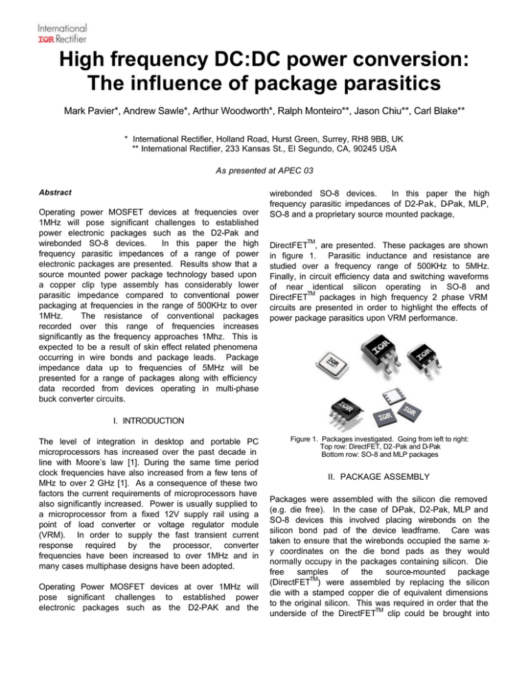
High frequency DC:DC power conversion: The influence of package parasitics Mark Pavier*, Andrew Sawle*, Arthur Woodworth*, Ralph Monteiro**, Jason Chiu**, Carl Blake** * International Rectifier, Holland Road, Hurst Green, Surrey, RH8 9BB, UK ** International Rectifier, 233 Kansas St., El Segundo, CA, 90245 USA As presented at APEC 03 Abstract Operating power MOSFET devices at frequencies over 1MHz will pose significant challenges to established power electronic packages such as the D2-Pak and wirebonded SO-8 devices. In this paper the high frequency parasitic impedances of a range of power electronic packages are presented. Results show that a source mounted power package technology based upon a copper clip type assembly has considerably lower parasitic impedance compared to conventional power packaging at frequencies in the range of 500KHz to over 1MHz. The resistance of conventional packages recorded over this range of frequencies increases significantly as the frequency approaches 1Mhz. This is expected to be a result of skin effect related phenomena occurring in wire bonds and package leads. Package impedance data up to frequencies of 5MHz will be presented for a range of packages along with efficiency data recorded from devices operating in multi-phase buck converter circuits. wirebonded SO-8 devices. In this paper the high frequency parasitic impedances of D2-Pak, D-Pak, MLP, SO-8 and a proprietary source mounted package, TM DirectFET , are presented. These packages are shown in figure 1. Parasitic inductance and resistance are studied over a frequency range of 500KHz to 5MHz. Finally, in circuit efficiency data and switching waveforms of near identical silicon operating in SO-8 and TM DirectFET packages in high frequency 2 phase VRM circuits are presented in order to highlight the effects of power package parasitics upon VRM performance. I. INTRODUCTION The level of integration in desktop and portable PC microprocessors has increased over the past decade in line with Moore’s law [1]. During the same time period clock frequencies have also increased from a few tens of MHz to over 2 GHz [1]. As a consequence of these two factors the current requirements of microprocessors have also significantly increased. Power is usually supplied to a microprocessor from a fixed 12V supply rail using a point of load converter or voltage regulator module (VRM). In order to supply the fast transient current response required by the processor, converter frequencies have been increased to over 1MHz and in many cases multiphase designs have been adopted. Operating Power MOSFET devices at over 1MHz will pose significant challenges to established power electronic packages such as the D2-PAK and the Figure 1. Packages investigated. Going from left to right: Top row: DirectFET, D2-Pak and D-Pak Bottom row: SO-8 and MLP packages II. PACKAGE ASSEMBLY Packages were assembled with the silicon die removed (e.g. die free). In the case of D-Pak, D2-Pak, MLP and SO-8 devices this involved placing wirebonds on the silicon bond pad of the device leadframe. Care was taken to ensure that the wirebonds occupied the same xy coordinates on the die bond pads as they would normally occupy in the packages containing silicon. Die free samples of the source-mounted package TM (DirectFET ) were assembled by replacing the silicon die with a stamped copper die of equivalent dimensions to the original silicon. This was required in order that the TM underside of the DirectFET clip could be brought into contact with the source electrode printed circuit board pads. Kelvin vias circuit Devices were assembled onto test cards fabricated from double-sided FR4 with 2 Ounce copper tracking. Sn62Pb36Ag2 near eutectic no clean solder (Multicore SN62MP100AGS90) was screen-printed onto test cards prior to component pick and place. After component placement test cards were re-flowed using a standard JEDEC profile and visually inspected for defects. Short circuit G D S Figures 2 from left to right III. TEST PROCEDURE Resistance and inductance measurements were performed using an Agilent/HP4285A high precision LCR meter. A custom designed test fixture was used to interface the device test cards to the LCR output current source/voltage sense (Kelvin) terminals. The test procedure was as follows: Note that the above procedure was carried out for each device at each frequency tested. The HP4285A was operated in the correction mode for improved low resistance repeatability. Figures 2(a), (b) and (c) show the OPEN circuit test card, short circuit test card, and TM device test card respectively, for the DirectFET package. It should be noted that in order to obtain low resistance short circuit measurements the Kelvin drain and source via holes were located as close together as possible. The resultant short circuit obtained between Kelvin vias was calculated to be in the region of 40 µOhms. Note that the track impedances from the Kevin vias to the device under test are included in all of the experimental results shown below. The results presented below are therefore for devices mounted on a board, not discrete devices. Figure 3 shows the test card designs for each of the packages investigated. The circle superimposed onto each of the images indicates the location of each of the sense vias. In each case these vias were located as close as possible to edge of the package, and where possible underneath the package leads. Figures 3 from left to right D2-Pak, D-Pak, SO-8, MLP and DirectFET T M test cards. Notes circles highlight sense via location. IV. PACKAGE RESISTANCE CHARACTERISTICS Figure 4 shows the board mounted package resistance versus frequency for each of the packages characterised. TM The DirectFET package shows the lowest board mounted package resistance from DC up to 5MHz. At frequencies of 1MHz and above it should be noted that surface mount devices based upon conventional leaded packages, such as the D2-Pak and D-Pak, show very significant increases in package resistance in relation to values measured at DC. Board mounted package resistance [mOhm] 1) Insert ‘open circuit test card’ into test fixture & perform OPEN circuit correction 2) Insert ‘short circuit test card’ into test fixture & measure SHORT circuit R and L values 3) Insert device test card into test fixture and measure LOAD R and L (a) OPEN, (b) SHORT and (c) DEVICE UNDER TEST Cards. 6.00 5.00 DFET 4.00 MLP 3.00 SO-8 D-Pak 2.00 D2-Pak 1.00 0.00 0 1 2 3 Frequency [MHz] 4 5 Figure 4. Measured package resistance versus frequency With reference to figure 4 each mounted package exhibits a characteristic increase in resistance with increasing frequency. This is expected to be a consequence of skin effect [2]. Skin effect is an electromagnetic phenomenon in which current flowing through a material of a given cross sectional area is confined to the perimeter of that area at elevated frequencies. For a flat plate of copper, or wire bond, for example, skin depth is given by the equation [2]: δ = (ρ/πµof)1/2 Where δ, is the skin depth in m, ρ is the material resistivity, µo is the permeability of free space and f, is frequency. Figure 5 shows the variation in skin depth with frequency for three common metals utilised in power electronics packaging; copper, aluminum and gold. At a frequency of 1MHz the skin depth for copper is approximately in the region of 60 um. This is significantly lower than the typical leadframe thickness of an SO-8 device for example, which is in the region of 250um. Figure 7 shows the board mounted die free package inductance versus frequency curves for a range of power electronic packages. Inductance in the source mounted TM DirectFET package is significantly lower than that of the more conventional wirebonded packages such as D2-Pak, D-Pak and SO-8. D2-Pak packages exhibit the highest inductance of all packages tested, exhibiting inductance values up to 5 times those measured for the TM DirectFET package. This is likely to be a consequence of the length of package leads and internal 15 mil aluminum wirebonds in the D2-Pak device. D-Pak packages, whilst not as high inductance as D2-Paks, also show inductance values significantly higher than TM SO-8, MLP and DirectFET packages. Again this is likely to be a consequence of the length of external package leads and internal 8 mil diameter Aluminum wires. 4.5 300.0 250.0 100 um Cu plate 250um Cu plate 4.0 25 um Au wire 3.5 Rac/Rdc The frequency dependence of the resistance and inductance of a rectangular shape of metal or circular cross section wire can be modelled using Maxwell’s equations. Resistance can be shown to be a function of the ratio of plate thickness, t, over skin depth, δ [3]. Figure 6 shows how the modelled resistances of plate and wire geometries vary with frequency. IV. PACKAGE INDUCTANCE CHARACTERISTICS 125 um Al wire 250um Al wire 3.0 375um Al wire 2.5 2.0 Skin depth [um] Skin depth Cu [um] 200.0 1.5 Skin depth Au [um] 150.0 1.0 Skin depth Al [um] 0 100.0 1 2 3 Frequency [MHz] 4 5 Figure 6. Modelled Rac/Rdc versus frequency for material geometries used in power electronic packaging. 50.0 0.0 0 1 2 3 4 5 6 7 8 9 10 Frequency [MHz] Figure 5. Skin depth of copper, aluminum and gold versus frequency With reference to figure 6 it can be seen that at 1MHz the ratio of AC to DC modelled resistance of a plate of 250um thickness is approximately 1.7. At higher frequencies the resistance ratio increases further as the AC resistance increases. Whilst these models are only approximations they highlight the effects skin depth has on typical materials used in electronic packaging at frequencies above 1MHz. The package inductance characteristics shown in figure 7 all show a decreasing trend in inductance with increasing frequency. Models based upon solving Maxwell’s equations for a uniform current density conductor have shown that the ratio of AC to DC inductance is also a function of the ratio of plate thickness to skin depth [3]. Board mounted package inductance [nH] 6.00 5.00 DFET MLP 4.00 SO-8 D-Pak 3.00 D2-Pak Package 2.00 1.00 0.00 0 1 2 3 Frequency [MHz] 4 5 Figure 8 shows the modelled inductance versus frequency for a range of electronic materials common in power electronic packaging. As with the resistance models the results are only approximate but highlight that the decreasing trend in inductance with frequency can be understood by applying Maxwell’s equations to simple geometries. With reference to figure 8 it can be shown that larger thickness geometries are expected to show an earlier onset to inductance change with frequency. It should be noted that this behaviour is not observed in figure 7 and further work is required to understand these phenomenon. 1.0 0.9 0.8 Board mounted die free package inductance [nH] 500KHz 4 MHz D2-Pak 2.0 5.0 5.0 4.8 D-Pak 2.6 4.9 2.4 2.3 SO-8 2.7 4.1 1.6 1.5 MLP 3.1 4.9 1.6 1.4 DirectFET T M 0.9 1.8 0.5 0.4 It should be re-affirmed at this point that that the die free package resistances presented in table 1 include contributions from circuit board routing underneath the package footprint of each mounted device. In the case of TM the DirectFET package the additional board parasitics and resistance of the copper dummy die add an estimated 0.6 mOhms to the DC die free package resistance. The actual die free package resistance is expected to be less than 100 µOhms. Board tracking contributions in the region of 0.5 mOhms may also be subtracted from the DC package resistances of the D2Pak, D-PAK, MLP and SO-8 device data. Extracting the board parasitics at above 500KHz however is more prone to error due to the presence of skin effects within the circuit tracking. For this reason the data presented above has not been corrected to remove the circuit board tracking parasitics present underneath each device. In many cases this can be considered a more realistic representation of package capability in circuit. V. EFFECT OF PACKAGE INDUCTANCE ON HIGH FREQUENCY VOLTAGE REGULATOR MODULE SWITCHING WAVEFORMS 0.7 100 um Cu plate 0.6 Board mounted die free package resistance [mOhm] 500kHz 4 MHz Table 1. Summary of package parasitics for power packages Figure 7. Board mounted package inductance versus frequency Lac/Ldc frequency over the range of 500KHz and 5MHz, producing a 20% and 12.5% drop in inductance respectively. D2-Pak and D-Pak devices show a 4% drop in inductance, whilst SO-8 shows a 6.25% drop over the frequency range measured. 250um Cu plate TM 25 um Au wire 0.5 125 um Al wire 0.4 250um Al wire 375um Al wire 0.3 0 1 2 3 4 5 Frequency [MHz] Figure 8. Modelled inductance versus frequency for a range of materials utilised in power electronic packages A summary of the package parasitic resistance and inductances measured at 500KHz and at 4MHz are TM shown below in table 1. DirectFET and MLP packages show the greatest change in package inductance with Switching waveforms of DirectFET and SO-8 packaged devices were measured in a 2-phase 1U VRM circuit operating at 500 KHz per phase. The VRM circuit is shown in figure 9. In order to highlight the effect of package parasitics on switching performance, silicon of the near identical active area, voltage and generation were used in both packages. Figure 10 shows a captured waveform of an SO-8 circuit switching 30 amps. Note the presence of inductance related ringing on the peak of the voltage trace. A similar waveform captured TM from a DirectFET circuit switching 30 amps is shown in figure 11. Figure 9. Image showing 2-phase 1U VRM design (0.5 MHz/phase) including heatsink attached to underside of board Comparing the waveforms in figure 10 and 11 it can be TM concluded that the DirectFET device produces considerably lower peak ringing voltages in circuit than that of the SO-8 device. The ratio of peak ringing voltages observed in each waveform can be used to estimate the ratio of inductances between the two packages by using the relationship V = LdI/dt, where I is the peak current being switched, L is the board mounted package inductance and dt is the switching rise time. The ratio of TM DirectFET to SO-8 inductance calculated using this approximation is 0.32, which is in very good agreement with the measured ratio of board mounted package inductances, 0.31 (0.5nH/1.6nH). Figure 10. In circuit Vds switching waveforms of SO-8 packaged device Figure 11. In circuit Vds switching waveforms of DirectFET T M packaged device TM VI. IN-CIRCUIT EFFICIENCY DATA OF DIRECTFET AND SO-8 DEVICES Prior work has shown 4 phase VRM’s constructed from TM DirectFET packages are capable of switching up to 120A at 1MHz [4,5]. Reducing the effects of package parasitics can be used to further increase the VRM operating frequency to 2 MHz. Figure 12 shows the TM efficiency versus frequency curves of DirectFET and SO-8 devices operating in 2-phase VRM circuits (as shown in figure 9). In both sets of devices tested the silicon technology and active areas were kept near TM identical. Both circuits containing SO-8 and DirectFET devices were cooled using a heatsink attached to the underside of the circuit boards. In both circuits a positive airflow of 400LFM was directed onto the heatsinks during recording of the efficiency data. The VRM circuits TM containing DirectFET packaged silicon show higher efficiencies than their SO-8 counterparts across the frequency spectrum measured. The difference in efficiency between the two circuits also increases with increasing frequency. This result reflects the reduced TM package parasitic losses in the DirectFET devices relative to those of the SO-8. It should be noted that the TM DirectFET packaged devices were also able to operate under higher load current conditions. For example at TM 1MHz the DirectFET VRM circuits were able to switch up to 60A whilst maintaining a board temperature of less than 100C. SO-8 devices were only able to switch in the region of 40A under identical operating conditions. The TM higher current handling capability of the DirectFET populated VRM circuits is attributable to the combination of lower package parasitics and the increased thermal TM performance of the DirectFET package. construction show similar trends. The trends in inductance observed are expected to be a consequence of skin effect phenomenon. 90% 88% DirectFET SO-8 Efficiency 86% 84% 82% 80% 78% 76% 0 0.5 1 1.5 2 2.5 Frequency [MHz] Figure 12. In circuit efficiency data versus frequency for SO-8 and DirectFET packaged silicon in 2-phase 1U VRM with 400LFM airflow TM The DirectFET package construction allows heat to be removed directly from the top of the package can assembly as well as through the can leads into the board [6,7]. This is referred to as ‘dual sided cooling’. In SO-8 packages, dual sided cooling is less efficient due to the presence of mold compound between the top surface of the silicon and the surrounding ambient. In this situation the majority of heat is removed from the silicon through the package leads into the circuit board. TM The DirectFET package has been shown to have the lowest board mounted resistance and inductance of the packages characterised. Efficiencies and switching TM waveforms of SO-8 and DirectFET packaged power MOSFET devices have been compared operating in VRM circuits. Comparison of drain to source voltage (VDS) switching waveforms between the two packages show that voltage ringing is significantly lower in TM DirectFET packaged devices compared to SO-8. The TM ratio of SO-8 to DirectFET board mounted package inductance values obtained experimentally using a precision LCR meter are in close agreement to values approximated from VDS switching waveform observations. TM VRM circuits assembled using DirectFET devices show significantly higher power efficiency in comparison to VRM circuits assembled using SO-8 packaged devices. TM The DirectFET based VRM circuits also show significantly increased current handling capability. This is due to the reduced package parasitics and improved TM thermal performance of the DirectFET package. VIII. [1] [2] [3] VII. CONCLUSIONS [4] Board mounted parasitic impedances of die free assemblies of D2-Pak, D-Pak, SO-8, MLP and the TM proprietary source mounted DirectFET power semiconductor packages have been experimentally determined over the frequency range of 500kHz to 5MHz. In all the packages characterised, package resistance is shown to increase significantly with frequency due to suspected skin effect phenomenon. Basic analytical modelling of assemblies used in power package construction has been demonstrated and results support the supposition that the increasing resistance trends are due to skin effects. Parasitic inductance has been shown to decrease with frequency over the range of 500KHz to 5MHz. Analytical modelling of simple assemblies used in power electronic package [5] [6] [7] REFERENCES Intel technology symposium, August 28th, 2002 Duffin, W.J., “Electricity and magnetism’, 4th Edition, McGraw Hill, p-372, 1990. S. Ramo, J. Whinnery, T. Van Duzer, “Fields and waves in communication electronics”, Wiley, 1994. R. Monteiro, C. Blake, A. Sawle, A. Woodworth, “High current voltage regulator module (VRM) uses DirectFET T M MOSFETs to achieve current densities of 25A/in2 at 1MHz to power 32 bit servers”, PSW conference, Chicago, Oct. 28th 2002. C. Blake, R. Monteiro, “Optimised gate drive voltage to achieve over 85% efficiency in a 4 phase 100A voltage regulator module (VRM)”, Intel Technology Symposium, Aug. 28th 2002 A. Sawle, C. Blake, D. Maric, “Novel power MOSFET packaging technology doubles power density In synchronousbuck converters for next generation microprocessors”, APEC 2002 conf. 11th – 13th March 2002, Dallas. A, Sawle, M.Standing, T.Sammon, A. Woodworth, ‘DirectFET: A proprietary new source mounted power package for board mounted power’, p-473, PCIM Europe Proceedings, July 19th – 21st, 2001, Nurnberg.
