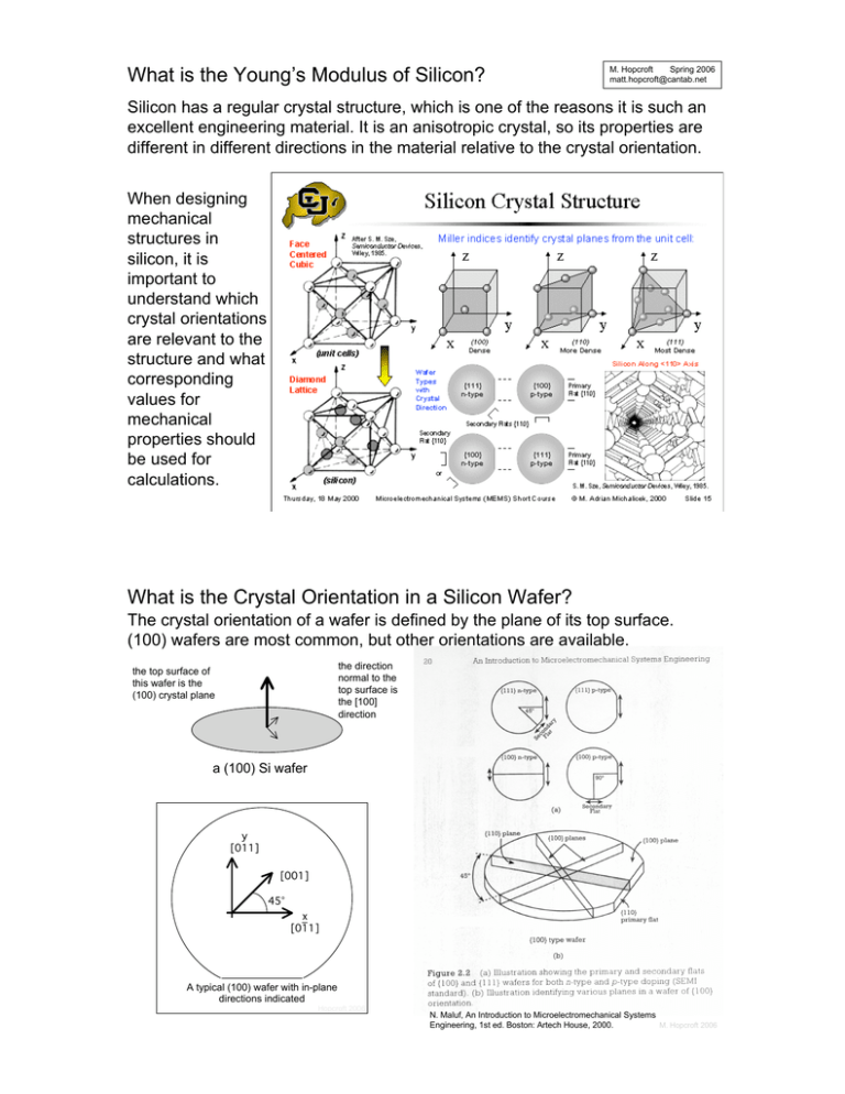
What is the Crystal Orientation in a Silicon Wafer?
advertisement

What is the Young’s Modulus of Silicon? M. Hopcroft Spring 2006 matt.hopcroft@cantab.net Silicon has a regular crystal structure, which is one of the reasons it is such an excellent engineering material. It is an anisotropic crystal, so its properties are different in different directions in the material relative to the crystal orientation. When designing mechanical structures in silicon, it is important to understand which crystal orientations are relevant to the structure and what corresponding values for mechanical properties should be used for calculations. M. Hopcroft 2006 What is the Crystal Orientation in a Silicon Wafer? The crystal orientation of a wafer is defined by the plane of its top surface. (100) wafers are most common, but other orientations are available. the direction normal to the top surface is the [100] direction the top surface of this wafer is the (100) crystal plane a (100) Si wafer y [011] [001] 45° x [011] A typical (100) wafer with in-plane directions indicated Hopcroft 2006 N. Maluf, An Introduction to Microelectromechanical Systems Engineering, 1st ed. Boston: Artech House, 2000. M. Hopcroft 2006 Fine. So What Value Should I Use for E of Silicon? • Silicon is an anisotropic crystal, so its Young’s modulus varies in different directions in the material relative to the crystal orientation. • Silicon has cubic symmetry, so the 3D direction-dependent properties can be described with a 6x6 matrix with only 3 independent constants (either stiffnesses Cij or compliances Sij). Because silicon is such an important economic material, these values have been investigated thoroughly. The best values of these constants are: C: 109 Pa S: 10-12 Pa Si C11 C12 C44 S11 S12 S44 165.7 63.9 79.6 7.68 -2.14 12.6 W. A. Brantley, "Calculated elastic constants for stress problems associated with semiconductor devices," Journal of Applied Physics, vol. 44, pp. 534-535, 1973. J. J. Wortman and R. A. Evans, "Youngs' Modulus, Shear Modulus and Poisson's Ratio in Silicon and Germanium," Journal of Applied Physics, vol. 36, pp. 153-156, 1965. H. J. McSkimin and J. P. Andreatch, "Elastic Moduli of Silicon vs Hydrostatic Pressure at 25.0 !C and - 195.8 ! C," Journal of Applied Physics, vol. 35, pp. 2161-2165, 1964. W. P. Mason, Physical acoustics and the properties of solids. Princeton, NJ USA: Van Nostrand, 1958. • For FEM calculations, use the stiffness matrix. Be sure to type it in yourself! Many common programs (ANSYS, FEMLAB) do not have default values.M. Hopcroft 2006 For design calculations: • Axial tension/compression: Use the E value for the direction of tension/compression. & 1 1 ) = S11 % 2(( S11 % S12 ) % S44 +( l 2 m 2 + m 2 n 2 + l 2 n 2 ) ' E "#$ 2 * ! 1 = S11 E100 1 1# 1 & = S11 " %( S11 " S12 ) " S44 ( E110 2$ 2 ' l = cos(" ) * m = cos(# ) n = cos($ ) 1 2# 1 & = S11 " %( S11 " S12 ) " S44 ( E111 3 $! 2 ' J. F. Nye, Physical properties of crystals : their representation by tensors and matrices. Oxford: Oxford University Press, 1985. * "direction cosines": cosine of the angle between the direction of interest and x,y,z axes (the <100> directions) ! • For example, in a (100) wafer: • for “x or y axis” (parallel to flat), use E110 = 169 GPa • for “off-axis” (45° diagonal to flat), use E100 = 130 GPa •Small deflection of a long, thin beam: This is basically axial tension and compression, so use the E value for the direction of the neutral axis. • Small deflection of a plate edge: Use a “plate modulus” for the major axis of bending: E "#$ , with Poisson’s ratio of ! = 0.28 for (100). [Brantley 1973] 1% & M. Hopcroft 2006 ! • Thin film stress/strain calculations for a thin film membrane or bending substrate (incl. Stoney’s equation calculations): Use the symmetric Biaxial modulus Bijk for the appropriate symmetric crystal plane, either (100) or (111) (the (110) plane is not symmetric). B100 = C11 + C12 " 2C12 C11 2 B111 = For example, B100 = 179.4 GPa 6C44 (C11 + 2C12 ) C11 + 2C12 + 4C44 W. D. Nix, Stanford MSE 353 Material Properties of Thin Films • For stress concentration calculations or multi-directional polycrystalline ! or Reuss volume average. ! situations (unusual), use a Voigt J. Diz and M. Humbert, "Practical aspects of calculating the elastic properties of polycrystals from the texture according to different models," Journal of Applied Crystallography, vol. 25, pp. 756-760, 1992. • For hydrostatic loads, use a Bulk modulus, B = 97.83 GPa. George, "Elastic constants and moduli of diamond cubic Si," in Properties of Crystalline Silicon, vol. 20, EMIS Datareviews, R. Hull, Ed. London: INSPEC, IEE, 1997, pp. 98. • Most silicon wafers are not pure silicon. Electronic doping changes the elastic behaviour in predictable ways. Typically the changes are negligible (1-5%). See J. J. Hall, "Electronic effects in the constants of n-type silicon," Physical Review, vol. 161, pp. 756, 1967, and references cited therein. For more information, see: •H. J. McSkimin, "Measurement of Elastic Constants at Low Temperatures by Means of Ultrasonic Waves--Data for Silicon and Germanium Single Crystals, and for Fused Silica," Journal of Applied Physics, vol. 24, pp. 988-997, 1953. •H. J. McSkimin, W. L. Bond, E. Buehler, and G. K. Teal, "Measurement of the Elastic Constants of Silicon Single Crystals and Their Thermal Coefficients," Physical Review, vol. 83, pp. 1080, 1951. •C. Bourgeois, E. Steinsland, N. Blanc, and N. F. de Rooij, "Design of resonators for the determination of the temperature coefficients of elastic constants of monocrystalline silicon," Proceedings of the 1997 IEEE International Frequency Control Symposium, 1997. •Stanford MSE 353 (Nix / Barnett) M. Hopcroft 2006 •Stanford MSE 208 (Dauskart)


