www.parallaxsemiconductor.com sa le s@pa ra lla xsemicondu ctor.c om sup port@p arallaxsemiconduc tor.c om ph on e: 916 ‐632 ‐46 64 • f a x:9 1 6‐62 4‐ 8003 Application Note AN008
Sigma-delta Analog to Digital Conversion
Abstract: Perform basic sigma-delta analog to digital conversion with any of the P8X32A's
eight cogs, on any pair of I/O pins, and with a few inexpensive passive components.
Variations on this simple technique include calibration options, multiple analog inputs,
converting from AC sources such as a microphone, and accommodating extended input
voltage ranges.
Introduction
Each of the Propeller’s eight cores, or cogs, has two configurable counter modules[1]. Each
of these modules, along with some external passive components, can be set up to do
analog-to-digital conversion using a “sigma-delta” technique. This is a method that keeps a
summing junction balanced by the rapid application of high and low logic levels and by
keeping track of how many such corrections it takes to maintain a constant voltage.
Sigma-Delta Principle
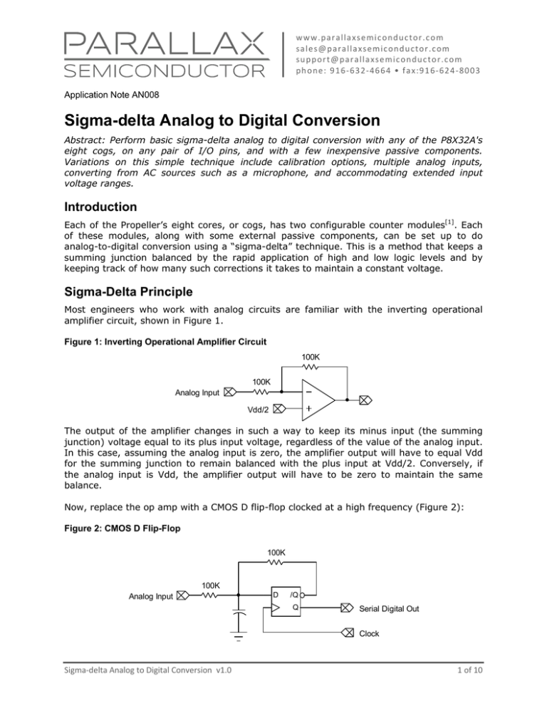
Most engineers who work with analog circuits are familiar with the inverting operational
amplifier circuit, shown in Figure 1.
Figure 1: Inverting Operational Amplifier Circuit
100K
100K
Analog Input
Vdd/2
The output of the amplifier changes in such a way to keep its minus input (the summing
junction) voltage equal to its plus input voltage, regardless of the value of the analog input.
In this case, assuming the analog input is zero, the amplifier output will have to equal Vdd
for the summing junction to remain balanced with the plus input at Vdd/2. Conversely, if
the analog input is Vdd, the amplifier output will have to be zero to maintain the same
balance.
Now, replace the op amp with a CMOS D flip-flop clocked at a high frequency (Figure 2):
Figure 2: CMOS D Flip-Flop
100K
100K
Analog Input
D
/Q
Q
Serial Digital Out
Clock
Sigma‐delta Analog to Digital Conversion v1.0 1 of 10
Parallax Semiconductor AN008 As in the case with the op amp, the negative feedback from the flip-flop (filtered by a cap
now) will tend to keep the summing junction as close to the D input’s logic threshold,
Vdd/2, as possible. If the analog input is zero volts, the /Q output will have to remain at
Vdd (i.e. logical one) for this to happen. Conversely, if the analog input is Vdd, the /Q
output will have to remain at Vss (i.e. logical zero). In between, the /Q pin will output a
digital pulse train whose average duty cycle is proportional to the amount of correction
required to keep the D input balanced at Vdd/2. If the analog input were Vdd/4, for
example, the /Q output would need to have a positive duty cycle of 75% to keep the D
input at Vdd/2.
To determine the value of the analog input voltage, it would only be necessary to measure
the duty cycle of the corrective /Q output. However, since /Q is inverted, it’s the Q
output’s duty cycle that is proportional to the analog input voltage. And this duty cycle can
be measured simply by counting the number of times the Q output is high for a given
number of clocks. This, then, is the essence of sigma-delta analog-to-digital conversion.
Propeller Sigma-Delta Application
Counter Registers
The Propeller provides the necessary hardware to perform sigma-delta analog-to-digital
conversions quite easily. To do so requires using the global count register, CNT, along with
one of the cog’s configurable counters. The global count register increments by one with
each “tick” of the internal clock, rolling over to zero after reaching a count of $FFFF_FFFF
(232 – 1). With an 80 MHz internal clock, one complete cycle of CNT takes about 53 seconds.
Each cog has two configurable counters. Each counter comprises three special-function
registers: CTRx, FRQx, and PHSx, where the “x” can be either A or B, depending on which
counter is referenced.
The CTRx register contents determine which counter mode and associated external ports
the counter uses. For sigma-delta operation, the counter mode is “positive with feedback.”
This means that the counter counts up for every clock cycle in which its input is a logic
“high.” It also means that the counter’s output pin will equal the inverse of its input pin,
delayed by one processor clock. Here is the layout of the CTRx register, configured for
sigma-delta operation (Figure 3):
Figure 3: CTRx Register Configured for Sigma-delta Operation
"Instruction" Field
31 30
26
"Destination" Field
23
01001
17
13
"Source" Field
9 8
Feedback Pin
4
0
Input Pin
Counter Mode
(Positive with Feedback)
The PHSx register accumulates the counter’s counts, counting up by the amount in FRQx at
each clock cycle in which the input pin is a logic high. Typically, for sigma-delta operation,
FRQx is set to one.
Configured in this manner, the counter mimics the behavior of the D flip-flop in Figure 2,
wherein the /Q output corresponds to the feedback pin and the Q output gates the upcounter.
Sigma‐delta Analog to Digital Conversion v1.0 2 of 10
Parallax Semiconductor AN008 Hardware Configuration
The circuit in Figure 2 represents an idealized situation, in which the logic threshold is
exactly Vdd/2 and in which the /Q high output is exactly Vdd and its low output, exactly 0.
Because these conditions seldom exist in reality, it is necessary to reduce the gain of the
circuit to less than unity in order to accommodate a full analog input range of 0 to Vdd.
Otherwise, the conversion could be clipped at the high or low end of the range. Figure 4
illustrates the circuit most commonly used with the Propeller to perform sigma-delta analogto-digital conversion:
Figure 4: Sigma-delta ADC Circuit
1 nF
150K
Analog Input
100K
Counter Output
Counter Input
1 nF
When the analog input is zero, the counter feedback output will have a nominal duty cycle
of 83.33%. When the input equals Vdd, the feedback’s nominal duty cycle will be 16.67%.
This provides enough of a margin at both extremes to accommodate the circuit variations
described above.
The circuit in Figure 4 includes a capacitor to Vdd, in addition to the one to ground. This is
done to prevent noise on the power and/or ground rails from affecting the voltage at the
summing junction asymmetrically, which could lead to sporadic conversion results.
Layout Considerations
For best performance, the passive components shown in Figure 4 should be positioned very
close to the Propeller’s input and feedback pins. The use of surface-mount components will
help to ensure that this objective is met. A typical layout is shown in Figure 5.
Sigma‐delta Analog to Digital Conversion v1.0 3 of 10
Parallax Semiconductor AN008 Figure 5: Typical Surface-Mount Layout
Also note from this photo that the corner of the chip package separates the counter input
and output pins. Using pins that are not physically adjacent helps to prevent capacitive
coupling from the output pin directly into the input pin.
Software Procedure
To set up the counter for sigma-delta operation, follow these steps:
1. Set FRQx to equal 1.
2. Set CTRx as shown in Figure 3.
3. Set the DIRA bit corresponding to the feedback pin to 1, thus making it an output.
To obtain an analog-to-digital conversion (in PASM), do this:
1.
2.
3.
4.
5.
Copy CNT to a variable, time, and add 16.
WAITCNT time, interval to sync (which also adds interval to time).
NEGate PHSx into the result register.
WAITCNT time for interval to pass.
ADD PHSx into the result register.
What this does is to sample how much PHSx has increased during interval processor
clocks. This increase will be proportional to the input voltage (plus an offset).
Sigma‐delta Analog to Digital Conversion v1.0 4 of 10
Parallax Semiconductor AN008 The following Propeller Assembly (PASM) code snippet illustrates the above steps.
'' Listing 1
CON
INP_PIN
FB_PIN
ADC_INTERVAL
= 8
= 9
= 512
'Counter input pin for sigma-delta.
'Counter feedback pin for sigma-delta.
'Time interval over which to accumulate counts.
DAT
org
mov
movi
movd
movs
mov
mov
0
frqa,#1
ctra,#%0_01001_000
ctra,#FB_PIN
ctra,#INP_PIN
dira,fb_mask
result_addr,par
'Initialize frqa to count up by one.
'Set ctra mode to positive w/feedback.
'Write fback pin number to dst field.
'Write input pin number to src field.
'Make the feedback pin an output.
'Save @value into result_addr.
main_loop
call
wrlong
jmp
#adc
acc,result_addr
#main_loop
'Get a new acquisition.
'Write result to hub.
'Back for another.
adc
time,cnt
time,#16
time,interval
acc,phsa
time,#0
acc,phsa
'Get the current counter value.
'Add a little to get ahead.
'Sync to clock; add interval to time.
'Negate phsa into result.
'Wait for interval to pass.
'Add phsa into result.
adc_ret
mov
add
waitcnt
neg
waitcnt
add
ret
fb_mask
result_addr
interval
long
long
long
1 << FB_PIN
0-0
ADC_INTERVAL
'Mask for feedback pin.
'Result address gets plugged in here.
'Acquisition time.
acc
time
res
res
1
1
'General-purpose accumulator.
'Time variable use for waitcnt.
adc_cog
Once the setup phase is complete, main_loop calls adc repeatedly and writes the result to a
pre-determined location in the hub. The PAR register specifies this location when the PASM
cog is started, via cognew:
cognew(@adc_cog, @value)
The scale factor of the result and the size of any offset will both be proportional to the
number used for interval. The magnitude of interval determines the precision of the
result. For eight bits of precision, say, interval would ideally equal 256; for nine bits, 512;
and so forth. In other words, for eight bits of precision, the PHSx register would contain a
count of how many times in 256 internal clocks the counter input was above the logic
threshold. But, because the input gain is less than unity, those eight bits will encompass
more than a 0-to-Vdd analog input range. Therefore, it will be necessary to increase the
value of interval to scale the desired input range to eight bits.
Calibration
For the most accurate results, it is necessary to calibrate the sigma-delta ADC to the high
and low endpoints of its input range. This requires that the ADC be presented with the
endpoint voltages in order to obtain readings from them. From a hardware standpoint, this
can be accomplished in several ways. If the analog device itself can output the endpoint
voltages, no additional hardware is necessary. If not, there are a couple techniques that will
Sigma‐delta Analog to Digital Conversion v1.0 5 of 10
Parallax Semiconductor AN008 work. In the typical case where the analog range is Vss to Vdd, the circuit in Figure 6 is
appropriate.
Figure 6: Calibration Circuit for Analog Range of Vss to Vdd
Calibration
100K
1 nF
R
Counter Output
150K
Analog Input
Counter Input
1 nF
In this circuit, an additional Propeller pin is used to provide the Vss and Vdd calibration
levels. The resistor R must be large enough not to overload the calibration pin or analog
source, but small enough not to skew the circuit’s gain once the calibration pin is tri-stated.
Another technique, which overcomes the limitations of the circuit in Figure 6, is to use an
analog multiplexer, as shown in Figure 7.
Figure 7: Analog Multiplexer
Vdd Calibrate Input
Analog Inputs
Ain0..3
4:1 Analog MUX
1 nF
150K
Aout
100K
Counter Output
Counter Input
S0 S1
1 nF
Vss Calibrate Input
Channel Select
Here, the calibration inputs can be selected at will without having to consider or compensate
for loading effects.
From a software standpoint, there are two approaches available for calibration. The simplest
is to pick a value for the sampling interval that is known to be larger than what is required
for the desired precision, then to scale the result based on the calibration data. This is
easiest if the scaling can be done in Spin, rather than PASM, after the raw ADC value is
acquired:
scaled := (raw - vlo) * RANGE / (vhi - vlo) #> 0 <# RANGE
In this expression, raw is the current raw sigma-delta reading, vlo is the raw reading for
the low-end calibration, vhi is the raw reading for the high-end calibration, and RANGE is the
highest value of the desired precision. This expression also clips the scaled value to lie
within the [0, RANGE] closed interval. Note that RANGE does not have to be a power of two; it
can be any positive number.
Sigma‐delta Analog to Digital Conversion v1.0 6 of 10
Parallax Semiconductor AN008 The two main disadvantages of this method are:
1. Unless interval is very large with respect to RANGE, the scaled result will exhibit
non-linearities in the least-significant bit due to unequal step sizes.
2. Since interval needs to be extra large, the conversion time is longer than it would
otherwise need to be.
The other technique is to determine ahead of time the value for interval that will produce
the desired precision with just an offset correction and no scaling. This involves successive
sampling of Vdd and Vss with candidate values of interval until the optimum value is
obtained. This technique lends itself to a binary search, such as that illustrated in Listing 2.
Notice in this listing that after each step change in the calibration output, the routine soak is
called. The soak delay (i.e. sample period) ensures that the analog input and counter
feedback have ample time to re-equalize due to the sudden input change before the next
acquisition. Also notice that in main_loop, after calling adc, the low reading (i.e. offset) gets
subtracted from the raw reading to yield the corrected reading. It may also be desirable at
this point to limit the corrected reading to the closed interval [0, range]. The maxs and mins
instructions can be employed to do this, after subtracting loresult:
maxs
mins
acc,range
acc,#0
Finally, although the code in this listing is geared toward the calibration circuit given in
Figure 6, it can easily be modified to accommodate the circuit of Figure 7 by toggling the
multiplexer channel select pins, instead of toggling the calibration pin up and down.
'' Listing 2
adc_cog
mov
movi
movd
movs
mov
mov
calibrate
or
mov
mov
shr
:searchlp
andn
call
call
mov
or
call
call
sub
cmp
if_z jmp
sumnc
shr
if_nz jmp
:got_it
main_loop
andn
call
sub
wrlong
frqa,#1
ctra,#%0_01001_000
ctra,#FB_PIN
ctra,#INP_PIN
dira,fb_mask
result_addr,par
'Initialize frqa to count up by one.
'Set ctra mode to positive w/feedback.
'Write fback pin number to dst field.
'Write input pin number to src field.
'Make the feedback pin an output.
'Save @value into result_addr.
dira,calib_mask
interval,interval0
dinterval,interval0
dinterval,#1
'Make calibration pin an output.
'Initialize acquisition interval.
'Initialize delta interval
' to interval/2.
outa,calib_mask
#soak
#adc
loresult,acc
outa,calib_mask
#soak
#adc
acc,loresult
acc,range wc,wz
#:got_it
'Output 0V on calibration pin.
'Delay to accommodate step change.
'Get the result.
'Save as the low value.
'Output Vdd on calibration pin.
'Delay to accommodate step change.
'Get the result.
'Subtract low value to get the range.
'Compare range with desired range.
'Done if spot on.
interval,dinterval
dinterval,#1 wz
#:searchlp
'Subtract if too high, add if too low.
'Cut delta interval in half.
'Done if now zero, loop if not.
dira,calib_mask
#adc
acc,loresult
acc,result_addr
'Done: tristate calibration pin.
'Get a new acquisition.
'Subtract the reading for 0V.
'Write result to hub.
Sigma‐delta Analog to Digital Conversion v1.0 7 of 10
Parallax Semiconductor AN008 jmp
#main_loop
'Back for another.
mov
add
waitcnt
ret
time,cnt
time,soak_time
time,#0
'Give the caps a chance to charge
' by waiting for soak time...
time,cnt
time,#16
time,interval
acc,phsa
time,#0
acc,phsa
'Get the current counter value.
'Add a little to get ahead.
'Sync to clock; add interval to time.
'Negate phsa into result.
'Wait for interval to pass.
'Add phsa into result.
adc_ret
mov
add
waitcnt
neg
waitcnt
add
ret
interval0
range
fb_mask
calib_mask
soak_time
result_addr
long
long
long
long
long
long
ADC_INTERVAL0
ADC_RANGE
1 << FB_PIN
1 << CALIB_PIN
40_000
0-0
'Initial acquisition interval.
'Desired ADC range.
'Mask for feedback pin.
'Mask for calibration pin.
'Sample (pre-soak) time for calib.
'Result address gets plugged in here.
interval
dinterval
acc
time
loresult
res
res
res
res
res
1
1
1
1
1
'Acquisition time.
'Delta interval for search.
'General-purpose accumulator.
'Time variable use for waitcnt.
'ADC raw result for low end of range.
soak
soak_ret
adc
Variations on a Theme
The sigma-delta technique lends itself to many variations that can be implemented to meet
specific needs, such as multiple inputs, inputs from AC sources (such as audio), and inputs
with extended voltage ranges.
Multiple Inputs
Multiple analog inputs can be accommodated with a single feedback pin
Figure 8: Multiple Analog Inputs
1 nF
150K
Analog Input 0
Counter Input 0
1 nF
100K
Counter Output
100K
1 nF
150K
Analog Input 1
Counter Input 1
1 nF
Sigma‐delta Analog to Digital Conversion v1.0 8 of 10
Parallax Semiconductor AN008 To switch from one input to another, reload the source field (bits 8..0) of CTRx with the new
input pin number. Although Figure 8 shows two analog inputs, this technique can be
extended to a larger number, as long as the passive components can be kept close to their
associated Propeller pins. The one major caveat is that, after switching inputs, it is
necessary to delay long enough before taking the first reading for the summing junction
caps on the new input to recharge to the input pin’s logic threshold. Also, when combined
with a need for calibration, it may be more advantageous from a pin count standpoint to use
an analog multiplexer, as shown in Figure 7.
Converting from AC Sources
The sigma-delta analog inputs do not need to be DC-coupled. For reading AC signals, such
as audio, capacitive coupling will also work, as shown in Figure 9. (This, by the way, is the
circuit used for the microphone input on the Propeller Demo Board[2].)
Figure 9: Capacitive Coupling for Reading AC Signals
Vdd
Vdd
10K
0.1uF
100K
1nF
Counter Output
+
Counter Input
Electret Mic.
1nF
Extended Voltage Ranges
The sigma-delta converter’s input range can be extended by choosing a larger input resistor
and/or by adding some biasing via a pull-up or pull-down resistor. In the “standard” circuit
with the 150 k input resistor, the nominal input voltage range (without considering offsets,
etc.) is -0.825 V to +4.125 V. Notice that this range centers around the input logic
threshold, which is nominally 1.65 V (Vdd/2) when Vdd is 3.3 V. To shift the center of the
range, it is necessary to add some biasing. For example, suppose the desired input range
were 0 to +10 V, which centers on +5 V. This would entail using a pull-down resistor on the
summing junction to re-center the range to 1.65 V, as shown in Figure 10.
Figure 10: Extended Voltage Ranges
1 nF
100K
Counter Output
R1
Analog Input
Counter Input
R2
1 nF
Sigma‐delta Analog to Digital Conversion v1.0 9 of 10
Parallax Semiconductor AN008 With the input at V HI = +10 V and the counter output at 0 V, the summing junction must
remain fixed at 1.65 V. Likewise, it must still be at 1.65 V when the input is at V LO = 0 V
and the counter output is 3.3 V. Computing R1 and R2 entails solving the following pair of
simultaneous equations:
VHI 1.65 1.65 1.65
Equation 1a
1.65 VLO 1.65 1.65
Equation 1b
R1
R1
R2
100
R2
100
w
...where the resistances are in k.
Solving these two equations for R1 and R2 yields:
R1
100VHI VLO
k
3.3
Equation 2a
R2
100VHI VLO
k
VHI VLO 3.3
Equation 2b
To guarantee that the entire 0-10 V range is covered without clipping at the high or low end
due to chip variations from the nominal input threshold, extend the limits above and below
the 5 V center value by about 50%, making the nominal range from –2.5 V to +12.5 V.
Plugging these values in for V LO and V HI , respectively, yields 455 k for R1 and 224 k for
R2.
If the result for R2 in the above equation is negative, simply change its sign and make it a
pull-up to Vdd, instead of a pull-down to Vss. If the computed value for R2 is infinite, just
leave it out entirely.
Resources
Listing 1 and Listing 2 code archives zip file: www.parallaxsemiconductor.com/an008
References
1. See AN001: Propeller P8X32A Counters; www.parallaxsemiconductor.com/an001
2. Propeller Demo Board; Parallax #32100, www.parallax.com
Revision History
Version 1.0: Original document.
Parallax, Inc., dba Parallax Semiconductor, makes no warranty, representation or guarantee regarding the suitability of its products
for any particular purpose, nor does Parallax, Inc., dba Parallax Semiconductor, assume any liability arising out of the application or
use of any product, and specifically disclaims any and all liability, including without limitation consequential or incidental damages
even if Parallax, Inc., dba Parallax Semiconductor, has been advised of the possibility of such damages. Reproduction of this
document in whole or in part is prohibited without the prior written consent of Parallax, Inc., dba Parallax Semiconductor.
Copyright © 2011 Parallax, Inc. dba Parallax Semiconductor. All rights are reserved.
Propeller and Parallax Semiconductor are trademarks of Parallax, Inc.
Sigma‐delta Analog to Digital Conversion v1.0 10 of 10


