28 dB Gain DC-6 GHz GaInP/GaAs HBT Wideband
advertisement
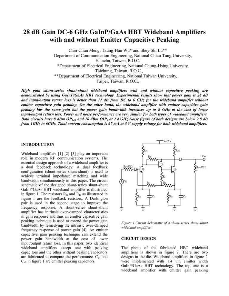
28 dB Gain DC-6 GHz GaInP/GaAs HBT Wideband Amplifiers with and without Emitter Capacitive Peaking Chin-Chun Meng, Tzung-Han Wu* and Shey-Shi Lu** Department of Communication Engineering, National Chiao Tung University, Hsinchu, Taiwan, R.O.C. *Department of Electrical Engineering, National Chung-Hsing University, Taichung, Taiwan, R.O.C., **Department of Electrical Engineering, National Taiwan University, Taipei, Taiwan, R.O.C., High gain shunt-series shunt-shunt wideband amplifiers with and without capacitive peaking are demonstrated by using GaInP/GaAs HBT technology. Experimental results show that power gain is 28 dB and input/output return loss is better than 12 dB from DC to 6 GHz for the wideband amplifier without emitter capacitive gain peaking. On the other hand, the wideband amplifier with emitter capacitive gain peaking has the same gain but the power gain bandwidth increases up to 8 GHz at the cost of lower input/output return loss. Power and noise performance are very similar for both types of wideband amplifiers. Both circuits have 8 dBm OP1dB and 20 dBm OIP3 at 2.4 GHz Noise figure of both designs are below 2.8 dB from 1GHz to 6GHz. Total current consumption is 67 mA at 5 V supply voltage for both wideband amplifiers. INTRODUCTION Wideband amplifiers [1] [2] [3] play an important role in modern RF communication systems. The essential design approach of a wideband amplifier is a dual feedback technology. A dual feedback configuration (shunt-series shunt-shunt) is used to achieve terminal impedance matching and wide bandwidth simultaneously in this paper. The circuit schematic of the designed shunt-series shunt-shunt GaInP/GaAs HBT wideband amplifier is illustrated in figure 1. The resistors Rf1 and Rf2 as illustrated in figure 1 are the feedback resistors. A Darlington pair is used in the second stage to improve the frequency response. A shunt-series shunt-shunt amplifier has intrinsic over-damped characteristics in gain response and thus an emitter capacitive gain peaking technique is used to extend the power gain bandwidth by remedying the intrinsic over-damped frequency response of power gain [4]. An emitter capacitive gain peaking technique can extend the power gain bandwidth at the cost of lower input/output return loss. In this paper, two identical wideband amplifiers except one with peaking capacitors and the other without peaking capacitors are fabricated to compare the performance. Ce1 and Ce2 in figure 1 are emitter peaking capacitors. Figure 1.Circuit Schematic of a shunt-series shunt-shunt wideband amplifier. CIRCUIT DESIGN The photo of the fabricated HBT wideband amplifiers is shown in figure 2. There are two designs in the die. Wideband amplifiers in figure 2 were implemented with 1.4 um emitter width GaInP/GaAs HBT technology. The top one is a wideband amplifier with emitter gain peaking 40 0 S21 with Capacitance S21 without Capacitance S21 (dB) 30 S11 (dB) capacitors and the bottom one is a wideband amplifier without emitter gain peaking capacitors. The bottom device layout has been rotated 180 degree with respect to the top one to facilitate onwafer probing. Both designs have identical transistor sizes for comparison purpose. The size of transistor Q1 is 1.4 µm x 9µm x 2, the size of transistor Q2 is 1.4µm x 6µm x 1 and the size of transistor Q3 is 1.4µm x 9µm x 5. The die size is 1 mm x 1 mm. Most of the die area is not fully utilized in order to facilitate the on-wafer measurement and fit the minimum die size requirement of the foundry service. The die size of each amplifier can be easily compacted into 0.4 mm x 0.4 mm. -10 20 -20 10 S11 with Capacitance S11 without Capacitance 0 -30 0 1 2 3 4 5 6 7 8 9 10 11 12 13 14 15 16 17 18 19 Frequency (GHz) Figure 3. Forward transmission gain and input return loss measurement results of wideband amplifiers with and without emitter capacitive gain peaking. S22 and S 12 (dB) 0 -10 S22 (with Capacitance) S22 (without Capacitance) -20 -30 -40 S12 (with Capacitance) S12 (without Capacitance) -50 0 1 2 3 4 5 6 7 8 9 10 11 12 13 14 15 16 17 18 19 Figure 2.Die Photo of shunt-series shunt-shunt wideband amplifiers with and without emitter capacitive gain peaking. RESULTS AND DISCUSSIONS Total current consumption is 67 mA at 5 V supply voltage for both wideband amplifiers during onwafer measurement. The first stage consumes 17 mA while the second stage consumes 50 mA. Forward transmission gain and input return loss are illustrated in figure 3 while reverse transmission gain and output return loss are illustrated in figure 4. The circuit without gain peaking capacitors has 6 GHz 3dB power gain bandwidth, S11 is below –15 dB and S22 is below –12 dB for the measurement range from DC to 18 GHz as revealed in figure 3 and figure 4. Frequency (GHz) Figure 4. Reverse transmission gain and output return loss measurement results of wideband amplifiers with and without emitter capacitive gain peaking. The circuit with emitter gain peaking capacitors has higher 3dB power gain bandwidth but suffers lower input/output return loss for frequencies above 4 GHz when gain peaking starts to show up. Thus, S11 reaches –8dB while S22 reaches –9 dB at 8 GHz for the circuit with emitter gain peaking capacitors. In other words, there exist some trade-offs between power gain bandwidth and matching bandwidth when emitter gain peaking capacitors are introduced. Figure 5 illustrates the ZT (50 Ω load transimpedance) and Z21 (open load transimpedance) of both two designs calculated from measured S parameters. The ZT is defined as the transimpedance gain with 50Ω load and is calculated according to the following widely used formula ZT = S 21 ⋅ 50 1 − S11 80 90 Z 21 with Capacitance Z 21 without Capacitance 80 ZT 60 Z21 60 50 50 40 Z T with Capacitance Z T without Capacitance 40 30 0 1 2 3 4 5 6 7 8 30 20 9 10 11 12 13 14 15 16 17 18 19 Frequency (GHz) Figure 5.Measured ZT & Z21 of wideband amplifiers with and without emitter capacitive peaking. 30 Output Power (dBm) 70 70 Z 21 (dB) Z T (dBΩ) Power performance is also measured. Both circuit have very similar power performance. 8 dBm OP1dB and 20 dBm OIP 3 at 2.4GHz are obtained for the circuit with emitter capacitive gain peaking as illustrated in figure 7. OP1dB and OIP3 of both circuits as a function of frequency are illustrated in figure 8. There is no apparent power performance difference between two designs. OIP3=20dBm 10 0 OP1dB=8dBm -10 -20 -30 -40 PF1 Power P2F1-F2 Power -50 -60 -40 The circuit using emitter gain peaking capacitors has 65 dBΩ gain and 8 GHz 3 dB bandwidth for ZT, but the circuit without emitter gain peaking capacitors has the same gain with 4 GHz 3 dB bandwidth for ZT. The Z21 data in figure 5 also shows that the emitter gain peaking capacitors has influence on Z21 response. -30 25 OIP 3 with capacitance OIP 3 without capacitance 20 15 10 5 0 OP 1dB with capacitance OP 1dB without capacitance -10 0 Noise Figure (dB) -10 Figure 7. Power performance at 2.4GH for the wideband amplifier with emitter gain peaking capacitor z -5 5.0 -20 Input Power (dBm) OP1dB and OIP3 Figure 6 illustrates the noise performance of both circuits. Noise figures of the two designs are below 2.8 dB for frequencies from 1 GHz to 6 GHz. Both designs have similar noise figures for frequencies up to 12 GHz and the wideband amplifier without emitter gain peaking capacitor shows slightly higher noise figures for higher frequencies. 20 1 2 3 Noise Figure (with capacitance) Noise Figure (without capacitance) 4.5 4 5 6 7 8 9 10 Frequency (GHz) 4.0 Figure 8. Power performance of wideband amplifiesr as a function of frequency 3.5 3.0 CONCLUSION 2.5 2.0 0 1 2 3 4 5 6 7 8 9 10 11 12 13 14 15 16 17 18 19 Frequency (GHz) Figure 6. Measured noise figures of wideband amplifiers with and without emitter capacitive gain peaking. 28 dB gain DC-6GHz GaInP/GaAs shunt-series shunt-shunt feedback wideband amplifiers are demonstrated in this paper. The experimental results show that power gain is 28 dB and input/output return loss is below 12 dB from DC to 6 GHz for the wideband amplifier without emitter capacitive 11 gain peaking. An emitter capacitive gain peaking technique can extend the 3dB power gain bandwidth at the cost of lower input/output return loss. The circuit using peaking capacitors has 8 GHz 3dB power gain bandwidth while S11 reaches –8dB and S22 reaches –9 dB at 8 GHz. Both circuits have similar noise and power performance. 8 dBm OP1dB and 20 dBm OIP3 at 2.4 GHz for both circuit are obtained. Noise figures of both circuits are below 2.8dB for frequencies from 1 GHz to 6 GHz. ACKNOWLEDGEMENT This work was supported by the National Science Council of Republic of China under grant NSC 90-2213E-005-001, grant NSC 90-2219-E-002-009 and by the Ministry of Education under grant 89-E-FA06-2-4. REFERENCES [1] Robert G. Meyer and Robert A. Blauschild, “A 4-Term wide-band monolithic amplifier,” IEEE Journal of Solid State Circuit, Vol. SC-16, No.6, pp. 634-638, Dec. 1981. [2] Christopher D. Hull and Robert G. Meyer, “Principles of monolithic wideband feedback amplifier design,” Int. Journal of High Speed Electronics, Vol. 3 No.1, pp.53-93, Feb. 1992. [3] K. W. Kobayashi aand A. K. Oki, “ A DC-10 GHz high gain-low noise GaAs HBT direct-coupled amplifier,” IEEE microwave and guide wave letters, Vol. 5 No. 9 Sep. 1995. [4] Ming-Chou Chiang, Shey-Shi Lu, Chin-Chun Meng, Shin-An Yu, Shih-Cheng Yang and Yi-Jen Chan, “Analysis, design, and optimization of InGaP-GaAs HBT matched-impedance wide-band amplifiers with multiple feedback loops,” IEEE Journal of Solid States Circuits, Vol. 37 No.6, pp.694-701, June 2002.
