AP8263
advertisement
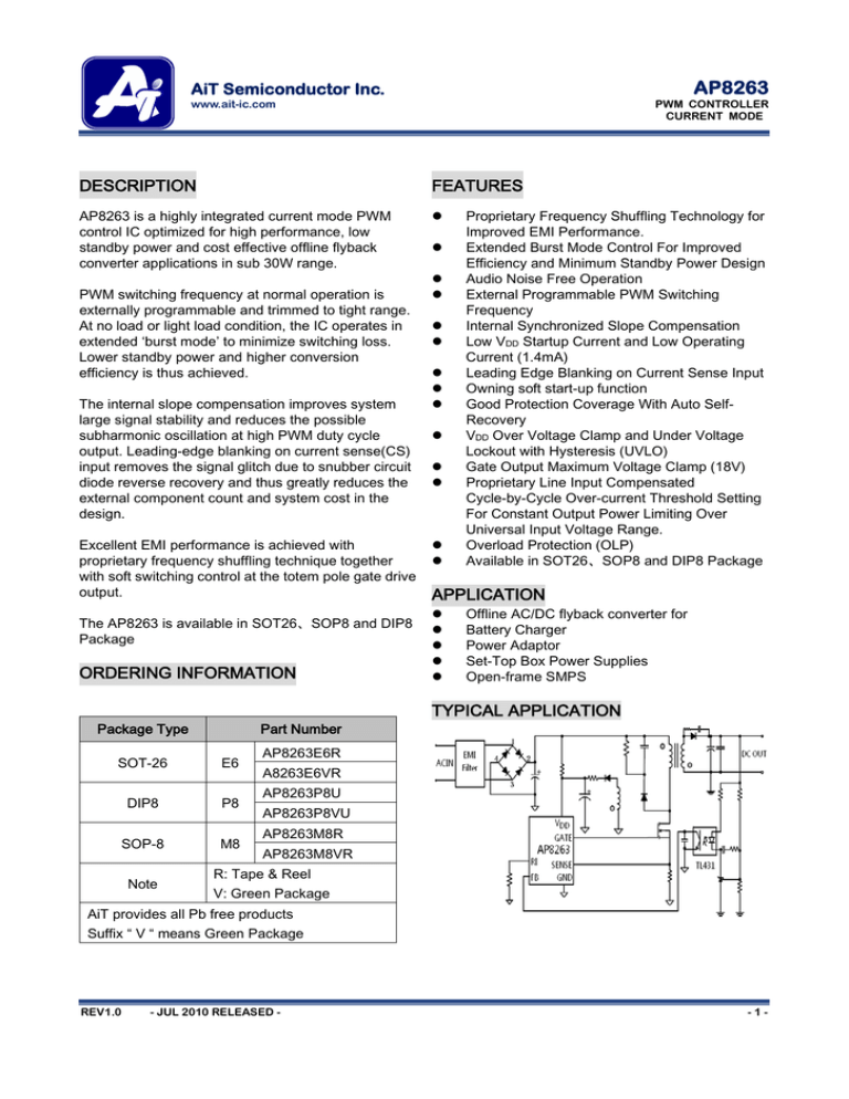
AP8263 AiT Semiconductor Inc. www.ait-ic.com PWM CONTROLLER CURRENT MODE DESCRIPTION FEATURES AP8263 is a highly integrated current mode PWM control IC optimized for high performance, low standby power and cost effective offline flyback converter applications in sub 30W range. PWM switching frequency at normal operation is externally programmable and trimmed to tight range. At no load or light load condition, the IC operates in extended ‘burst mode’ to minimize switching loss. Lower standby power and higher conversion efficiency is thus achieved. The internal slope compensation improves system large signal stability and reduces the possible subharmonic oscillation at high PWM duty cycle output. Leading-edge blanking on current sense(CS) input removes the signal glitch due to snubber circuit diode reverse recovery and thus greatly reduces the external component count and system cost in the design. Excellent EMI performance is achieved with proprietary frequency shuffling technique together with soft switching control at the totem pole gate drive output. The AP8263 is available in SOT26、SOP8 and DIP8 Package ORDERING INFORMATION Package Type Part Number SOT-26 E6 DIP8 P8 SOP-8 M8 Note Proprietary Frequency Shuffling Technology for Improved EMI Performance. Extended Burst Mode Control For Improved Efficiency and Minimum Standby Power Design Audio Noise Free Operation External Programmable PWM Switching Frequency Internal Synchronized Slope Compensation Low VDD Startup Current and Low Operating Current (1.4mA) Leading Edge Blanking on Current Sense Input Owning soft start-up function Good Protection Coverage With Auto SelfRecovery VDD Over Voltage Clamp and Under Voltage Lockout with Hysteresis (UVLO) Gate Output Maximum Voltage Clamp (18V) Proprietary Line Input Compensated Cycle-by-Cycle Over-current Threshold Setting For Constant Output Power Limiting Over Universal Input Voltage Range. Overload Protection (OLP) Available in SOT26、SOP8 and DIP8 Package APPLICATION Offline AC/DC flyback converter for Battery Charger Power Adaptor Set-Top Box Power Supplies Open-frame SMPS TYPICAL APPLICATION AP8263E6R A8263E6VR AP8263P8U AP8263P8VU AP8263M8R AP8263M8VR R: Tape & Reel V: Green Package AiT provides all Pb free products Suffix “ V “ means Green Package REV1.0 - JUL 2010 RELEASED - -1- AP8263 AiT Semiconductor Inc. www.ait-ic.com PWM CONTROLLER CURRENT MODE PIN DESCRIPTION Top View Top View Pin # Symbol SOT-26 DIP8 SOP-8 1 8 8 GND 2 7 7 FB 3 5 5 RI 4 4 4 SENSE 5 2 2 VDD 6 1 1 GATE 3,6 3,6 NC REV1.0 - JUL 2010 RELEASED - Top View Function Ground Feedback input pin. The PWM duty cycle is determined by voltage level into this pin and SENSE pin input. Internal Oscillator frequency setting pin. A resistor connected between RI and GND sets the PWM frequency. Current sense input pin. Connected to MOSFET current sensing resistor node. Chip DC power supply pin. Totem-pole gate drive output for the power MOSFET. -2- AiT Semiconductor Inc. www.ait-ic.com AP8263 PWM CONTROLLER CURRENT MODE ABSOLUTE MAXIMUM RATINGS VDD to GND Voltage 28V VDD Clamp Current 10mA VDD Clamp Voltage 28V VFB, VSENSE and VRI to GND Voltage -0.3V to + 7V Junction temperature -20°C to + 150° Storage Temperature -55°C to + 160°C VDD Voltage RI Resistor Value Operating Ambient Temperature Human body mode Machine mode 10V to + 27V 100kOhm -20°C to + 85°C 2000V 200V Stresses above may cause permanent damage to the device. These are stress ratings only and functional operation of the device at these or any other conditions beyond those indicated in the Electrical Characteristics are not implied. Exposure to absolute maximum rating conditions for extended periods may affect device reliability. NOTE: Do not exceed these limits to prevent damage to the device. Exposure to absolute maximum rating conditions for long periods may affect device reliability. REV1.0 - JUL 2010 RELEASED - -3- AP8263 AiT Semiconductor Inc. www.ait-ic.com PWM CONTROLLER CURRENT MODE ELECTRICAL CHARACTERISTICS TA = 25°C if not otherwise specified Parameter Symbol Conditions Min Typ Max Unit - 3 20 uA - 1.4 - mA UVLO(ON) 7.8 8.8 9.8 V UVLO(OFF) 13 14 15 V IVDD = 5mA - 28 - V ΔVFB /ΔVCS - 2.0 - V/V - 4.8 - V - 1.2 - mA - - 0.75 V VTH_PL - 3.7 - V TD_PL - 35 - mSec Input Impedance ZFB_IN - 4 - Kohm Maximum Duty Cycle DC_MAX - 75 - % Supply Voltage (VCC) VDD =12.5V, RI=100K VDD Start up Current I_VDD_Startup Measure Leakage current into VDD Operation Current I_VDD_Ops VDD Under Voltage Lockout Enter VDD Under Voltage Lockout Exit (Recovery) VDD Zener Clamp Voltage VDD_Clamp VDD=16V, RI=100Kohm, VFB=3V Feedback Input Section(FB Pin) PWM Input Gain AVCS VFB Open Loop Voltage VFB_Open FB pin short circuit current IFB_Short Zero Duty Cycle FB Threshold Voltage Power Limiting FB Threshold Voltage Power limiting Debounce Time REV1.0 - JUL 2010 RELEASED - VTH _0D Short FB pin to GND and measure current VDD = 16V, RI=100Kohm VDD=18V, RI=100Kohm, FB=3V, CS=0 -4- AP8263 AiT Semiconductor Inc. www.ait-ic.com Parameter PWM CONTROLLER CURRENT MODE Symbol Conditions Min Typ Max Unit Current Sense Input(Sense Pin) Leading edge blanking time T_blanking Input Impedance ZSENSE_IN Over Current Detection and Control Delay Over Current Threshold Voltage at zero Duty Cycle Soft-start up time TD _OC VTH _OC RI = 100Kohm VDD = 16V, CS>VTH_OC, FB=3.3V FB=3.3V, RI=100Kohm tSS - 300 - ns - 40 - Kohm - 75 - nSec 0.70 0.75 0.80 V - 2 - ms 60 65 70 KHz - 5 - % - 5 - % 50 100 150 Kohm - 2 - V - 22 - KHz Oscillator Normal Oscillation FOSC Frequency Frequency Temperature Stability RI = 100Kohm VDD Δf_Temp = 16V, RI=100Kohm, TA -20 ℃ to 100℃ Frequency Voltage Stability Δf_VDD Operating RI Range RI_range RI open load voltage V_RI_open Burst Mode Base Frequency FOSC_BM VDD = 12-25V, RI=100Kohm VDD = 16V, RI = 100Kohm Gate Drive Output Output Low Level VOL VDD=16V, IO=-20mA - - 0.8 V Output High Level VOH VDD=16V, IO=20mA 10 - - V Output Clamp V_Clamp - 18 - V Output Rising Time T_r VDD=16V, CL=1nf - 220 - nSec Output Falling Time T_f VDD=16V, CL=1nf - 70 - nSec Frequency Δf_OSC RI=100K -3 - 3 % Shuffling Frequency f_shuffling RI=100K - 64 - Hz Frequency Shuffling REV1.0 - JUL 2010 RELEASED - -5- AP8263 AiT Semiconductor Inc. www.ait-ic.com PWM CONTROLLER CURRENT MODE TYPICAL PERFORMANCE CHARACTERISTICS VDD = 16V, RI = 100Kohm, TA = 25℃ condition applies if not otherwise specified 1. VDD UVLO and Operation Current 2. I_start vs. VDD 3. I_op vs. GATE Loading 4. Fosc(KHz) vs RI(Kohm) 5. Duty vs.VDD 6. VG_Clamp vs. VDD REV1.0 - JUL 2010 RELEASED - -6- AP8263 AiT Semiconductor Inc. www.ait-ic.com PWM CONTROLLER CURRENT MODE 7. I_FB_Short vs.VDD 8. I_op vs. VDD 9. V_FB_open vs.VDD 10. V_RI vs.VDD 11. VTH_OC(V) vs Duty_cycle(%) REV1.0 - JUL 2010 RELEASED - -7- AiT Semiconductor Inc. www.ait-ic.com AP8263 PWM CONTROLLER CURRENT MODE BLOCK DIAGRAN REV1.0 - JUL 2010 RELEASED - -8- AiT Semiconductor Inc. www.ait-ic.com AP8263 PWM CONTROLLER CURRENT MODE DETAILED INFORMATION The AP8263 is a highly integrated PWM controller IC optimized for offline flyback converter applications in sub 30W power range. The extended burst mode control greatly reduces the standby power consumption and helps the design easily meet the international power conservation requirements. Startup Current and Start up Control Startup current of AP8263 is designed to be very low so that VDD could be charged up above UVLO threshold level and device starts up quickly. A large value startup resistor can therefore be used to minimize the power loss yet provides reliable startup in application. For AC/DC adaptor with universal input range design, a 2 MΩ, 1/8 W startup resistor could be used together with a VDD capacitor to provide a fast startup and low power dissipation solution. Operating Current The Operating current of AP8263 is low at 1.4mA. Good efficiency is achieved with AP8263 low operating current together with extended burst mode control features. Soft-Start up During the converter start up time, the primary current limitation is progressively increased to the maximum value. In this way the stress on the secondary diode is considerably reduced. it also help to prevent transformer saturation. The soft-start up time lasts 2 ms and the featuer is implemented for every attempt of start up converter. Frequency shuffling for EMI improvement The frequency Shuffling/jittering (switching frequency modulation) is implemented in AP8263. The oscillation frequency is modulated with a random source so that the tone energy is spread out. The spread spectrum minimizes the conduction band EMI and therefore reduces system design challenge. Extended Burst Mode Operation At zero load or light load condition, majority of the power dissipation in a switching mode power supply is from switching loss on the MOSFET transistor, the core loss of the transformer and the loss on the snubber circuit. The magnitude of power loss is in proportion to the number of switching events within a fixed period of time. Reducing switching events leads to the reduction on the power loss and thus conserves the energy. REV1.0 - JUL 2010 RELEASED - -9- AiT Semiconductor Inc. www.ait-ic.com AP8263 PWM CONTROLLER CURRENT MODE AP8263 self adjusts the switching mode according to the loading condition. At from no load to light/medium load condition, the FB input drops below burst mode threshold level. Device enters Burst Mode control. The Gate drive output switches only when VDD voltage drops below a preset level and FB input is active to output an on state. Otherwise the gate drive remains at off state to minimize the switching loss and reduces the standby power consumption to the greatest extend. The frequency control also eliminates the audio noise at any loading conditions. Oscillator Operation A resistor connected between RI and GND sets the constant current source to charge/discharge the internal cap and thus the PWM oscillator frequency is determined. The relationship between RI and switching frequency follows the below equation within the specified RI in Kohm range at nominal loading operational condition. Current Sensing and Leading Edge Blanking Cycle-by-Cycle current limiting is offered in AP8263 current mode PWM control. The switch current is detected by a sense resistor into the sense pin. An internal leading edge blanking circuit chops off the sense voltage spike at initial MOSFET on state due to Snubber diode reverse recovery so that the external RC filtering on sense input is no longer required. The current limit comparator is disabled and thus cannot turn off the external MOSFET during the blanking period. PWM duty cycle is determined by the current sense input voltage and the FB input voltage. Internal Synchronized Slope Compensation Built-in slope compensation circuit adds voltage ramp onto the current sense input voltage for PWM generation. This greatly improves the close loop stability at CCM and prevents the sub-harmonic oscillation and thus reduces the output ripple voltage. Gate Drive AP8263 Gate is connected to an external MOSFET gate for power switch control. Too weak the gate drive strength results in higher conduction and switch loss of MOSFET while too strong gate drive output compromises the EMI. A good tradeoff is achieved through the built-in totem pole gate design with right output strength and dead time control. The low idle loss and good EMI system design is easier to achieve with this REV1.0 - JUL 2010 RELEASED - - 10 - AiT Semiconductor Inc. www.ait-ic.com AP8263 PWM CONTROLLER CURRENT MODE dedicated control scheme. An internal 18V clamp is added for MOSFET gate protection at higher than expected VDD input. Protection Controls Good power supply system reliability is achieved with its rich protection features including Cycle-by- Cycle current limiting (OCP), Over Load Protection (OLP) and over voltage clamp, Under Voltage Lockout on VDD (UVLO). With Proprietary technology, the OCP threshold tracks PWM Duty cycles and is line voltage compensated to achieve constant output power limit over the universal input voltage range with recommended reference design. At overload condition when FB input voltage exceeds power limit threshold value for more than TD_PL, control circuit reacts to shut down the output power MOSFET. Device restarts when VDD voltage drops below UVLO limit. VDD is supplied by transformer auxiliary winding output. It is clamped when VDD is higher than threshold value. The power MOSFET is shut down when VDD drops below UVLO limit and device enters power on start-up sequence thereafter. REV1.0 - JUL 2010 RELEASED - - 11 - AP8263 AiT Semiconductor Inc. www.ait-ic.com PWM CONTROLLER CURRENT MODE PACKAGE INFORMATION Dimension in SOT-26 (Unit: mm) Symbol A A1 A2 b c D E E1 e e1 L θ REV1.0 - JUL 2010 RELEASED - Min 1.050 0.000 1.050 0.300 0.100 2.820 1.500 2.650 0.950(BSC) 1.800 0.300 0° Max 1.250 0.100 1.150 0.500 0.200 3.020 1.700 2.950 2.000 0.600 8° - 12 - AP8263 AiT Semiconductor Inc. www.ait-ic.com PWM CONTROLLER CURRENT MODE Dimension in SOP-8 (Unit: mm) Symbol Min Max A 1.350 1.750 A1 0.100 0.250 A2 1.350 1.550 b 0.330 0.510 c 0.170 0.250 D 4.700 5.100 E 3.800 4.000 E1 5.800 6.200 e REV1.0 - JUL 2010 RELEASED - 1.270(BSC) L 0.400 1.270 θ 0° 8° - 13 - AP8263 AiT Semiconductor Inc. www.ait-ic.com PWM CONTROLLER CURRENT MODE Dimension in DIP8 (Unit: mm) Symbol Min Max A 3.710 4.310 A1 0.510 - A2 3.200 3.600 B 0.380 0.570 B1 C 0.204 0.360 D 9.000 9.400 E 6.200 6.600 E1 7.320 7.920 e REV1.0 - JUL 2010 RELEASED - 1.524(BSC) 2.540(BSC) L 3.000 3.600 E2 8.400 9.000 - 14 - AP8263 AiT Semiconductor Inc. www.ait-ic.com PWM CONTROLLER CURRENT MODE IMPORTANT NOTICE AiT Semiconductor Inc. (AiT) reserves the right to make changes to any its product, specifications, to discontinue any integrated circuit product or service without notice, and advises its customers to obtain the latest version of relevant information to verify, before placing orders, that the information being relied on is current. AiT Semiconductor Inc.'s integrated circuit products are not designed, intended, authorized, or warranted to be suitable for use in life support applications, devices or systems or other critical applications. products in such applications is understood to be fully at the risk of the customer. Use of AiT As used herein may involve potential risks of death, personal injury, or servere property, or environmental damage. In order to minimize risks associated with the customer's applications, the customer should provide adequate design and operating safeguards. AiT Semiconductor Inc. assumes to no liability to customer product design or application support. AiT warrants the performance of its products of the specifications applicable at the time of sale. REV1.0 - JUL 2010 RELEASED - - 15 -


