HV450
Ordering Information
Operating Voltage
Package Options
VNN1
SOW-16
-220V
HV450WG
Features
General Description
Integrated high voltage transistors
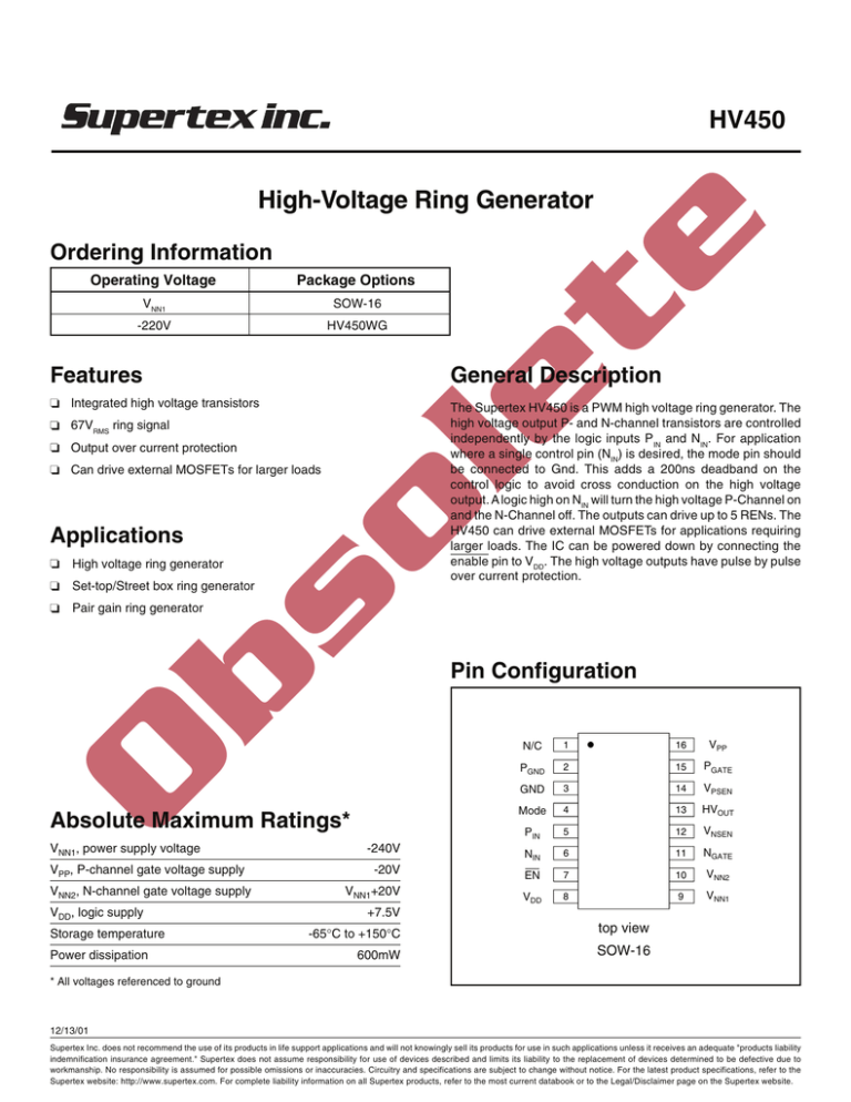
The Supertex HV450 is a PWM high voltage ring generator. The
high voltage output P- and N-channel transistors are controlled
independently by the logic inputs PIN and NIN. For application
where a single control pin (NIN) is desired, the mode pin should
be connected to Gnd. This adds a 200ns deadband on the
control logic to avoid cross conduction on the high voltage
output. A logic high on NIN will turn the high voltage P-Channel on
and the N-Channel off. The outputs can drive up to 5 RENs. The
HV450 can drive external MOSFETs for applications requiring
larger loads. The IC can be powered down by connecting the
enable pin to VDD. The high voltage outputs have pulse by pulse
over current protection.
67VRMS ring signal
ol
Output over current protection
Can drive external MOSFETs for larger loads
Applications
High voltage ring generator
bs
Set-top/Street box ring generator
et
e
High-Voltage Ring Generator
Pair gain ring generator
O
Pin Configuration
Absolute Maximum Ratings*
VNN1, power supply voltage
VPP, P-channel gate voltage supply
VNN2, N-channel gate voltage supply
VDD, logic supply
Storage temperature
Power dissipation
-240V
N/C
1
16
VPP
PGND
2
15
PGATE
GND
3
14
VPSEN
Mode
4
13
HVOUT
PIN
5
12
VNSEN
NIN
6
11
NGATE
-20V
EN
7
10
VNN2
VNN1+20V
VDD
8
9
VNN1
+7.5V
-65°C to +150°C
top view
600mW
SOW-16
* All voltages referenced to ground
12/13/01
Supertex Inc. does not recommend the use of its products in life support applications and will not knowingly sell its products for use in such applications unless it receives an adequate "products liability
indemnification insurance agreement." Supertex does not assume responsibility for use of devices described and limits its liability to the replacement of devices determined to be defective due to
workmanship. No responsibility is assumed for possible omissions or inaccuracies. Circuitry and specifications
are subject to change without notice. For the latest product specifications, refer to the
1
Supertex website: http://www.supertex.com. For complete liability information on all Supertex products, refer to the most current databook or to the Legal/Disclaimer page on the Supertex website.
HV450
Electrical Characteristics
(Over operating supply voltages unless otherwise specified, TA = -40°C to +85°C.)
Symbol Parameters
Min
Typ
Max
Unit
VPP
P-channel linear regulator output voltage
-10
-18
V
VNN1
High voltage negative supply
- 220
-110
V
VNN2
Negative linear regulator output voltage VNN1 + 6.0
VNN1 + 10.0
V
VDD
Logic supply voltage
5.5
V
INN1Q
VNN1 quiescent current
300
500
IDDQ
VDD1 quiescent current
90
200
35
100
4.5
25
INN1
VNN1 operating current
IDD
VDD operating current
IIL
Mode logic input low current
VIL
Logic input low voltage
0
VIH
Logic input high voltage
4.0
1.4
µA
µA
mA
1.0
25
Conditions
PIN = NIN = EN = L
PIN = NIN = L, EN = H
PIN = NIN = EN = L
PIN = NIN = L, EN = H
No load, VOUTP and VOUTN switching at
100KHz
mA
µA
Mode = 0V
1.0
V
VDD = 5.0V
5.0
V
VDD = 5.0V
Max
Unit
High Voltage Output
Symbol Parameters
Min
Typ
Conditions
RSOURCE VOUTP source resistance
65
Ω
IOUT = 100mA
RSINK
VOUTP sink resistance
65
Ω
IOUT = -100mA
td(ON)
HVOUT delay time
150
ns
PIN = high to low, Mode = high
trise
HVOUT rise time
50
ns
PIN = high to low
td(OFF)
HVOUT delay time
200
ns
NIN = low to high, Mode = high
tfall
HVOUT fall time
50
ns
NIN = low to high
tdb
Logic deadband time
250
ns
Mode = low
Vpsen
HVOUT current source sense voltage
Vnsen
HVOUT current sink sense voltage
tshortP
HVOUT off delay time when current
source sense is activiated
HVOUT off delay time when current sink
sense is activated
tshortN
-1.2
-0.8
V
VNN1 + 0.8
VNN1 + 1.2
V
70
150
ns
70
150
ns
twhout
Minimum pulse width for HVOUT at PGND
500
ns
twlout
Minimum pulse width for HVOUT at VNN1
500
ns
Truth Table
NIN
PIN
Mode
EN
HVOUT
L
L
H
L
Pgnd
L
H
H
L
High Z
H*
L*
H
L
*
H
H
H
L
VNN1
L
X
L
L
VNN1
H
X
L
L
Pgnd
X
X
X
H
High Z
*This state will short VNN1 to Pgnd and should therefore be avoided.
2
HV450
Block Diagram
PGND
High
Voltage
Level
Translator
VDD
PIN
NIN
EN
Mode
Current
Sense
and
Driver
Pgate
Linear
Reg
VPP
Logic
GND
Vpsen
HVOUT
VDD
Linear
Reg
High
Voltage
Level
Translator
VNN2
Ngate
Current
Sense
and
Driver
Vnsen
VNN1
Pin Description
VPP
P-channel gate voltage supply. Generated by an internal linear regulator. A 0.1µF capacitor should be connected between
PGND and VPP.
VNN1
Negative high voltage supply.
VNN2
N-channel gate voltage supply. Generated by an internal linear regulator. A 0.1µF capacitor should be connected between
VNN2 and VNN1.
VDD
Logic supply voltage.
GND
Low voltage ground.
PGND
High voltage power ground.
PIN
Logic control input. When mode is high, logic input high turns OFF output high voltage P-Channel.
NIN
Logic control input. When mode is high, logic input high turns ON output high voltage N-Channel.
EN
Logic enable input. Logic low enables IC.
Mode
Logic mode input. Logic low activates 200nsec deadband. When mode is low, NIN turns on and off the high voltage N- and
P-Channels. Pin is not used and should be connected to VDD or ground.
HVOUT
High voltage output. Voltage swings from PGND to VNN1.
Vpsen
Pulse by pulse over current sensing for P-Channel MOSFET.
Vnsen
Pulse by pulse over current sensing for N-Channel MOSFET.
Pgate
Gate drive for external P-channel MOSFET.
Ngate
Gate drive for external N-channel MOSFET.
3
HV450
Typical Application Circuit
Pgnd
Feedback
Network
3.9Ω
High
Voltage
Level
Translator
VDD
PIN
Current
Sense
and
Driver
Linear
Reg
EN
0.1µF
Pgate
VPP
HVOUT
NIN
µ-Controller
Vpsen
10mH
Logic
VDD
Mode
GND
High
Voltage
Level
Translator
Sine Wave
Ring Output
0.22µF
VNN2
Linear
Reg
Ngate
Current
Sense
and
Driver
0.1µF
Vnsen
3.9Ω
VNN1
HV450
12/13/010
©2001 Supertex Inc. All rights reserved. Unauthorized use or reproduction prohibited.
4
1235 Bordeaux Drive, Sunnyvale, CA 94089
TEL: (408) 744-0100 • FAX: (408) 222-4895
www.supertex.com


